Display device and binding test method thereof

A technology for testing display devices and chips, which is used in identification devices, static indicators, instruments, etc., can solve the problems of increasing the difficulty of pin technology and increasing the risk of ion migration of pins, so as to reduce the migration rate and improve the Ion migration phenomenon, effect of reducing difficulty

Active Publication Date: 2022-06-17
WUHAN TIANMA MICRO ELECTRONICS CO LTD
View PDF8 Cites 0 Cited by
  • Summary
  • Abstract
  • Description
  • Claims
  • Application Information

AI Technical Summary

Problems solved by technology

[0003] However, after the test is over, the test pins of the circuit board will be idle on the flexible circuit board as useless pins. Due to the large number of test pins on the circuit board, in the case of limited pin setting space, it can only be reduced. Small spacing between pins, or reducing the width of the pins, will not only increase the difficulty of the pin formation process, but also increase the risk of ion migration between the pins

Method used


Image

  • Display device and binding test method thereof
  • Display device and binding test method thereof
  • Display device and binding test method thereof

Examples


Embodiment Construction

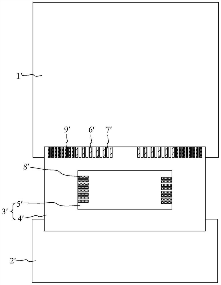
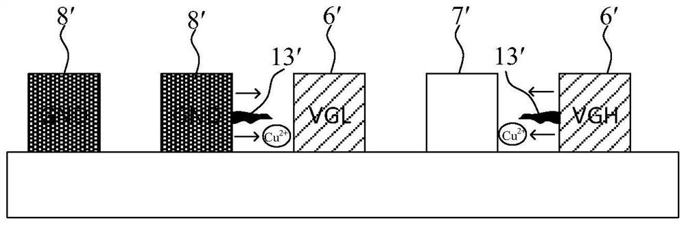
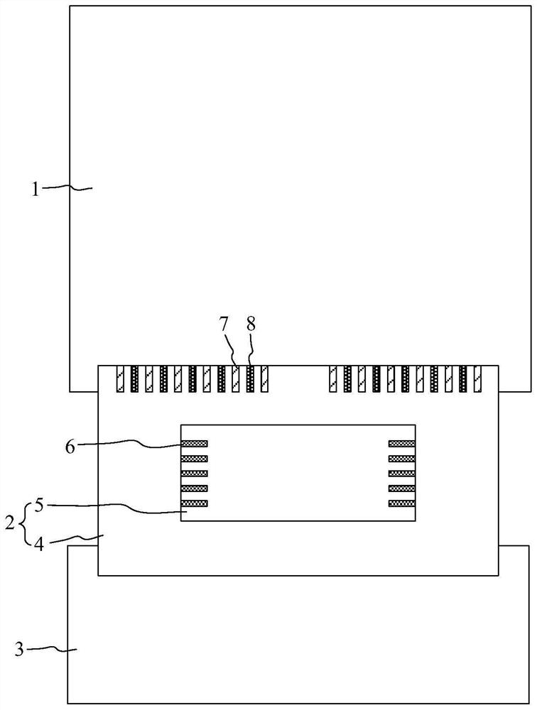
[0029] In order to better understand the technical solutions of the present invention, the embodiments of the present invention are described in detail below with reference to the accompanying drawings.

[0030] It should be understood that the described embodiments are only some, but not all, embodiments of the present invention. Based on the embodiments of the present invention, all other embodiments obtained by those of ordinary skill in the art without creative efforts shall fall within the protection scope of the present invention.

[0031] The terms used in the embodiments of the present invention are only for the purpose of describing specific embodiments, and are not intended to limit the present invention. As used in the embodiments of the present invention and the appended claims, the singular forms "a," "the," and "the" are intended to include the plural forms as well, unless the context clearly dictates otherwise.

[0032] It should be understood that the term "an...


PUM


Abstract

Embodiments of the present invention provide a display device and a binding test method thereof, which reduce the difficulty of the pin formation process and the risk of ion migration between the pins. The display device includes a display panel, a chip-on-chip film and a printed circuit board, and the chip-on-chip film includes a flexible circuit board and a driver chip; the driver chip includes chip test pins; the flexible circuit board includes functional pins and floating pins, and the functional pins It is used to transmit the signals required for the display screen of the display panel or the signals required for the operation of the driving chip; the chip test pins are led to the flexible circuit board through the floating pins; at least one floating pin is located between two adjacent functional pins ;In the non-test phase, the floating pin is in the high impedance state or the signal output state, when the floating pin is in the signal output state, the potential of the signal output by the floating pin is greater than the first potential V1 and lower than the second potential V2, the first potential V1 and the second potential V2 are respectively potentials of two functional pins adjacent to the floating pin.

Description

【Technical field】 [0001] The present invention relates to the field of display technology, and in particular, to a display device and a binding test method thereof. 【Background technique】 [0002] Chip On Film (COF) refers to a die soft film that fixes a driver chip on a flexible circuit board, and this structure is widely used in many types of display devices. After binding the driver chip on the flexible circuit board, in order to test the binding of the driver chip, the driver chip needs to reserve some pins as the chip test pins, and this part of the chip test pins is led out through the circuit board test pins. On the flexible circuit board of the chip-on-film, during the test process, test signals are provided to the test pins of the circuit board, and the potential of the test pins of the chip is detected to determine whether the driver chip is well bound. [0003] However, after the test, the circuit board test pins will be idle on the flexible circuit board as usel...

Claims


Application Information

Patent Timeline
Patent Type & Authority Patents(China)
IPC IPC(8): G09G3/00G09G3/20G09F9/00
CPCG09G3/006G09G3/20G09F9/00
Inventor 吴瀚巩厚富梁帝李涛刘畅梁振华黄杨
Owner WUHAN TIANMA MICRO ELECTRONICS CO LTD
Why Eureka
Try Eureka