Array substrate, display panel and display device

A technology for array substrates and display panels, which is applied in the fields of array substrates, display panels, and display devices, can solve the problems of unfavorable narrow frame design of display panels, increase in the number of signal lines, etc., and achieve narrow frame design, increase the number of settings, and good The effect of conductivity

Active Publication Date: 2020-12-25
XIAMEN TIANMA MICRO ELECTRONICS
View PDF15 Cites 3 Cited by
  • Summary
  • Abstract
  • Description
  • Claims
  • Application Information

AI Technical Summary

Problems solved by technology

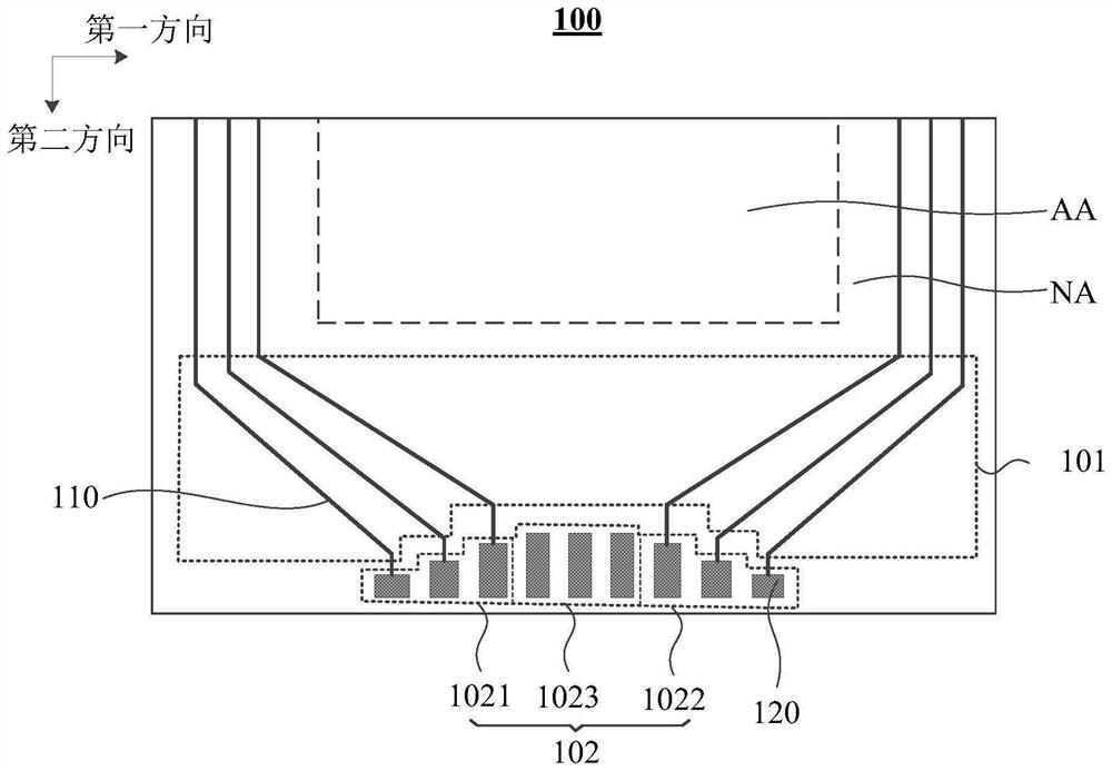
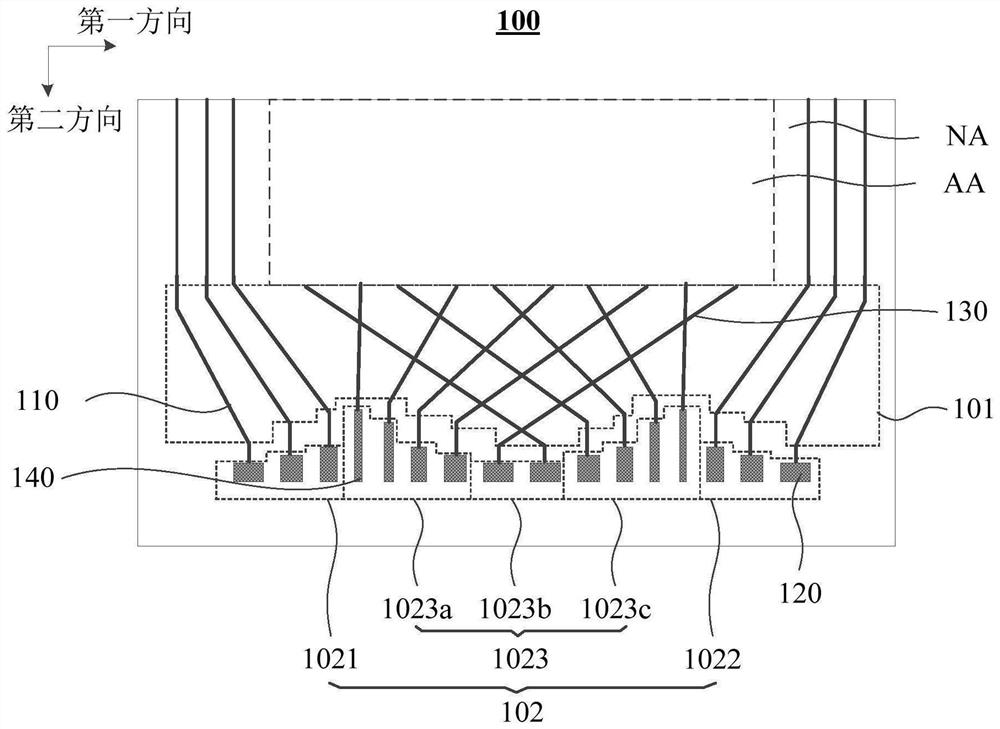
[0003] The existing display screen with integrated in-screen fingerprint recognition, due to the added fingerprint recognition function, needs to set up the signal wiring related to the fingerprint recognition module, which leads to an increase in the number of signal wiring on the array substrate, so more space is required for setting Signal routing, which is not conducive to the narrow bezel design of the display panel

Method used


Image

  • Array substrate, display panel and display device
  • Array substrate, display panel and display device
  • Array substrate, display panel and display device

Examples


Embodiment Construction

[0023] The application will be further described in detail below in conjunction with the accompanying drawings and embodiments. It should be understood that the specific embodiments described here are only used to explain the present application, but not to limit the present application. In addition, it should be noted that, for the convenience of description, only some structures related to the present application are shown in the drawings but not all structures.

[0024] In the prior art, the fingerprint recognition function is added to the display panel of the integrated in-screen fingerprint recognition, which requires additional signal wiring on the array substrate, which increases the number of signal wiring on the array substrate. Allow more room for signal routing. This results in an increase in the width of the non-display area of ​​the array substrate, which is not conducive to narrow frame design.

[0025] In order to solve the above technical problems, an embodim...


PUM


Abstract

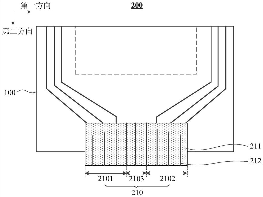
The invention discloses an array substrate, a display panel and a display device. The array substrate comprises a display area and a non-display area surrounding the display area, wherein the non-display area comprises a fan-out area and a binding area; the fan-out area is located between the binding area and the display area; the fan-out area is provided with a plurality of first connecting lines; the binding area is provided with a plurality of first binding terminals; the first connecting wires are electrically connected with the first binding terminals in a one-to-one correspondence manner; the first binding terminals are arranged along a first direction; in the first direction, the binding area comprises a first area and/or a second area and a third area, and the first area and the second area are located on the two opposite sides of the third area; the plurality of first binding terminals are located in the first area and/or the second area; in the first direction, the lengths ofthe plurality of first binding terminals in the binding area are gradually reduced from the center to the two sides, and the widths of the plurality of first binding terminals are gradually increasedfrom the center to the two sides. The embodiment of the invention is beneficial to realizing a narrow frame design.

Description

technical field [0001] The present invention relates to the field of display technology, in particular to an array substrate, a display panel and a display device. Background technique [0002] Fingerprint identification technology is one of the most widely used biometric identification technologies. Applying it to smart terminals can realize functions such as smart unlocking and online payment. The fingerprint identification module and the display panel can be prepared separately, and the fingerprint identification module is fixed on the outside of the display panel to form a display screen for fingerprint identification on the integrated screen; the fingerprint identification module and the display panel can also be prepared at the same time, and the fingerprint identification module is arranged on the display panel. Inside the panel, a display screen with integrated in-screen fingerprint recognition is easily formed. Because the latter has a smaller thickness, its product...

Claims


Application Information

Patent Timeline
Patent Type & Authority Applications(China)
IPC IPC(8): G09F9/30
CPCG09F9/30
Inventor 杨栩刘博智陈国照
Owner XIAMEN TIANMA MICRO ELECTRONICS
Why Eureka
Try Eureka