Semiconductor wafer surface cleaning and safe storage protection box

A surface cleaning and protection box technology, which is applied in semiconductor/solid-state device manufacturing, transportation and packaging, conveyor objects, etc., can solve the problems of damaged wafer circuit, wafer damage, loss, etc., and achieve the effect of reducing vibration

Inactive Publication Date: 2020-12-25
深圳市云陌科技有限公司
View PDF0 Cites 3 Cited by
  • Summary
  • Abstract
  • Description
  • Claims
  • Application Information

AI Technical Summary

Problems solved by technology

[0002] After the semiconductor wafer is etched, there will be scraps remaining in the gaps in the circuit. Using a traditional brush will damage the circuit on the surface of the wafer. Moreover, the wafer is relatively thin and difficult to pick up by hand. Excessive force will damage the wafer. Cause losses, the wafer needs to be stored, transported and transported after the etching is completed. The vibration generated by the general storage device during the operation will cause the wafer to shake, causing damage to the wafer and affecting the quality of the wafer. In severe cases, it may cause relatively large losses

Method used


Image

  • Semiconductor wafer surface cleaning and safe storage protection box
  • Semiconductor wafer surface cleaning and safe storage protection box
  • Semiconductor wafer surface cleaning and safe storage protection box

Examples


Embodiment Construction

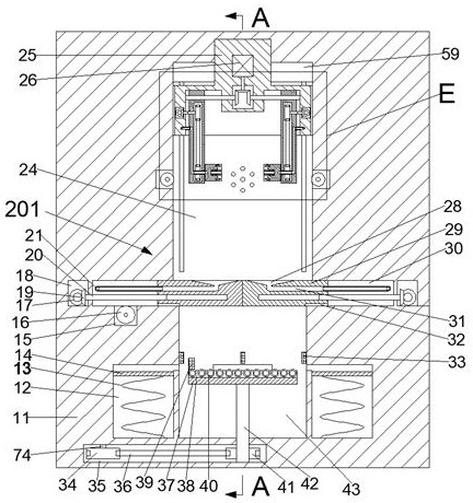
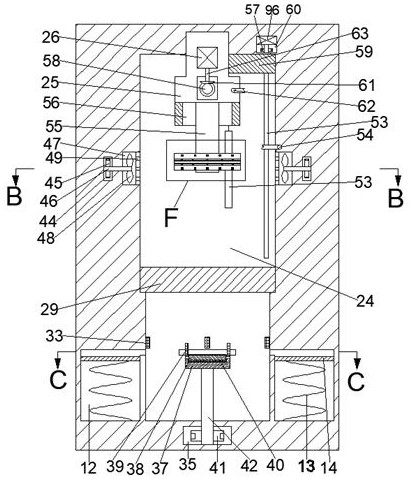
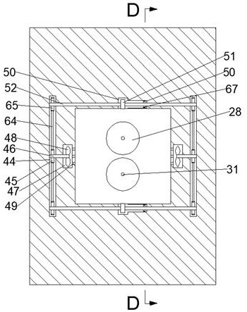
[0025] Combine below Figure 1-9 The present invention is described in detail, wherein, for the convenience of description, the orientations mentioned below are defined as follows: figure 1 The up, down, left, right, front and back directions of the projection relationship itself are the same.

[0026]A semiconductor wafer surface cleaning and safe storage protection box according to the present invention includes a box body 11, a lifting cavity 24 is arranged inside the box body 11, and a clip is provided for sliding up and down between the left and right walls of the lifting cavity 24. Holding block 25, the clamping block 25 is provided with a clamping plate cavity 56 with an opening downward, and the left and right walls of the clamping plate cavity 56 slide left and right and are symmetrically provided with a clamping plate 55. The plate 55 is rotatably connected to one end face and is provided with a rotating block 23. The rotating block 23 is provided with a clamping ca...


PUM


Abstract

The invention discloses a semiconductor wafer surface cleaning and safe storage protection box, which comprises a box body, wherein a lifting cavity is formed in the box body, a clamping block is arranged between the left wall and the right wall of the lifting cavity in an up-down sliding mode, and a clamping plate cavity with a downward opening is formed in the clamping block. According to the invention, the etched semiconductor wafers are washed, dried and stored, some sweeps exist in gaps of the etched wafers, due to the fact that the sweeps are small and difficult to remove, after the etched wafers are clamped by the device, cleaning liquid is sprayed, the sweeps in the gaps fall off by rotating the wafers and turning over the wafers, a drying device blows off the sweeps and dries thewafers, the processed wafers are stored in storage cavities respectively, and a damping device in the storage box can reduce vibration generated by movement of the device, so that the storage environment of the wafers is stable, and the wafers are prevented from being damaged by vibration.

Description

technical field [0001] The invention relates to the semiconductor field, in particular to a semiconductor wafer surface cleaning and safe storage protection box. Background technique [0002] After the semiconductor wafer is etched, there will be scraps remaining in the gaps in the circuit. Using a traditional brush will damage the circuit on the surface of the wafer. Moreover, the wafer is relatively thin and difficult to pick up by hand. Excessive force will damage the wafer. Cause losses, the wafer needs to be stored, transported and transported after the etching is completed. The vibration generated by the general storage device during the operation will cause the wafer to shake, causing damage to the wafer and affecting the quality of the wafer. In severe cases, it may cause relatively large losses. A semiconductor wafer surface cleaning and safe storage protection box described in the present invention can solve the above problems. Contents of the invention [0003...

Claims


Application Information

Patent Timeline
Patent Type & Authority Applications(China)
IPC IPC(8): H01L21/673H01L21/677H01L21/687H01L21/67
CPCH01L21/67034H01L21/67051H01L21/67356H01L21/67369H01L21/67763H01L21/68764H01L21/68792
Inventor 温妖
Owner 深圳市云陌科技有限公司
Why Eureka
Try Eureka