Method for improving poor bubbles of QFN bottom bonding pad and bonding pad
A technology of bottom pads and pads, applied in the electronic field, can solve problems affecting chip heat dissipation and PCBA reliability, and achieve the effects of improving reliability, reducing large bubbles, and ensuring conductivity
- Summary
- Abstract
- Description
- Claims
- Application Information
AI Technical Summary
Problems solved by technology
Method used
Image
Examples
Embodiment Construction
[0017] The preferred embodiments of the present invention will be described in detail below in conjunction with the accompanying drawings, so that the advantages and features of the present invention can be more easily understood by those skilled in the art, so as to define the protection scope of the present invention more clearly.
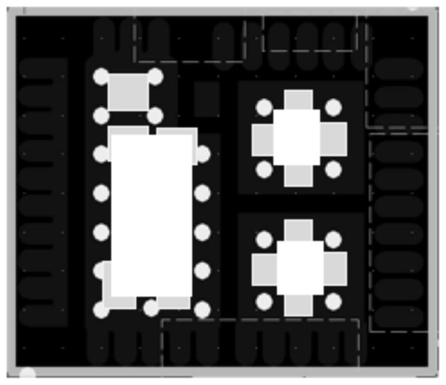
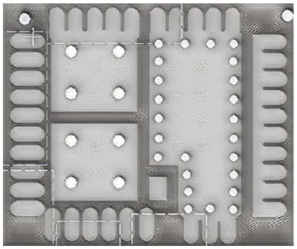
[0018] see figure 1 with figure 2 , the embodiment of the present invention includes:
[0019] See figure 1 , a method for improving the bad air bubbles of the QFN bottom pad, including: designing the position of the Via hole according to the shape of the QFN pad, canceling the Via hole in the middle of the pad, and appropriately adding some Via holes on the edge of the pad according to the actual size of the pad To meet the conductivity of PCBA. It can not only reduce the occurrence rate of air bubbles but also keep you ventilating and dissipating heat. In addition, it can better improve the poor air bubbles. According to the pad design of ...
PUM
| Property | Measurement | Unit |
|---|---|---|
| Aperture | aaaaa | aaaaa |
Abstract
Description
Claims
Application Information


