Novel FPGA chip layout optimization method

A chip layout and optimization method technology, applied in the field of FPGA, can solve the problems of adjustment, poor flexibility, and difficult adjustment of adjustment weights, etc., and achieve the effect of flexible debugging process, strong adaptability and pertinence, and avoiding limitations

Active Publication Date: 2021-01-05
WUXI ESIONTECH CO LTD +1
View PDF4 Cites 0 Cited by
  • Summary
  • Abstract
  • Description
  • Claims
  • Application Information

AI Technical Summary

Problems solved by technology

[0004] In the process of debugging the layout, it is necessary to continuously adjust the influence of each cost function on the layout optimization objective function, so that the layout result can be obtained under the premise of optimizing the layout optimization objective function value, but in the actual debugging process
The current method is to adjust the period influence by adjusting the weight of each cost function during the iterative process, but this adjustment method is not flexible. In this case, it is difficult to adjust the influence of each cost function correctly only by adjusting the weight; in addition, adjusting the weight can only make indiscriminate adjustments to the influence of the sa

Method used


Image

  • Novel FPGA chip layout optimization method
  • Novel FPGA chip layout optimization method

Examples


Embodiment Construction

[0031] The specific embodiments of the present invention will be further described below in conjunction with the accompanying drawings.

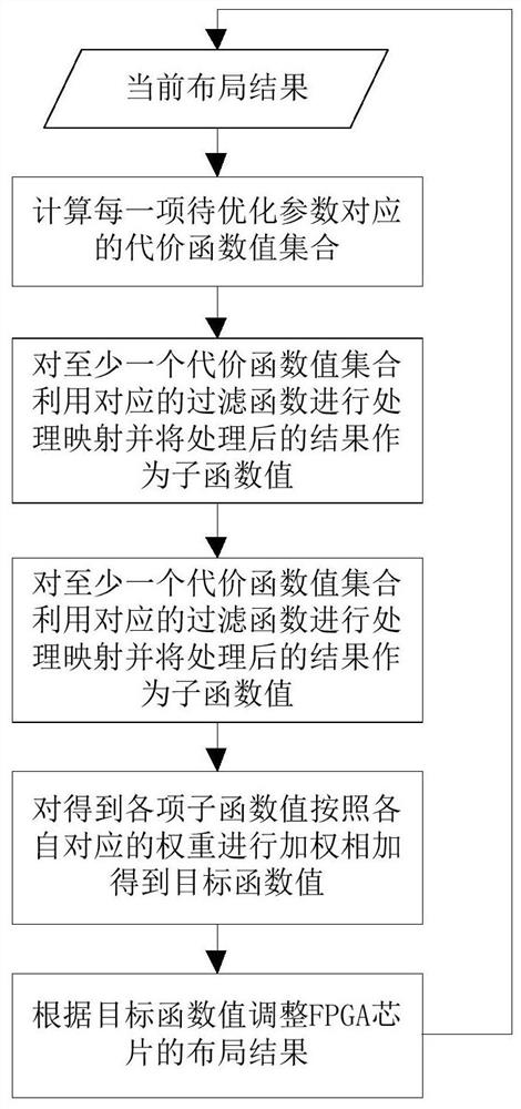
[0032] This application discloses a novel FPGA chip layout optimization method, the method includes the following steps, please refer to figure 1 :

[0033] Step S1, calculating a set of cost function values ​​corresponding to each parameter to be optimized under the current layout of the FPGA chip. Among them, the parameters to be optimized include wire length (NET WIRELENGTH), total wire length (TOTAL WIRELENGTH), path timing margin (SLACK), wire congestion (CONGESTION), power consumption distribution (POWER), clock tree range ( at least one of CLOCKSPAN).

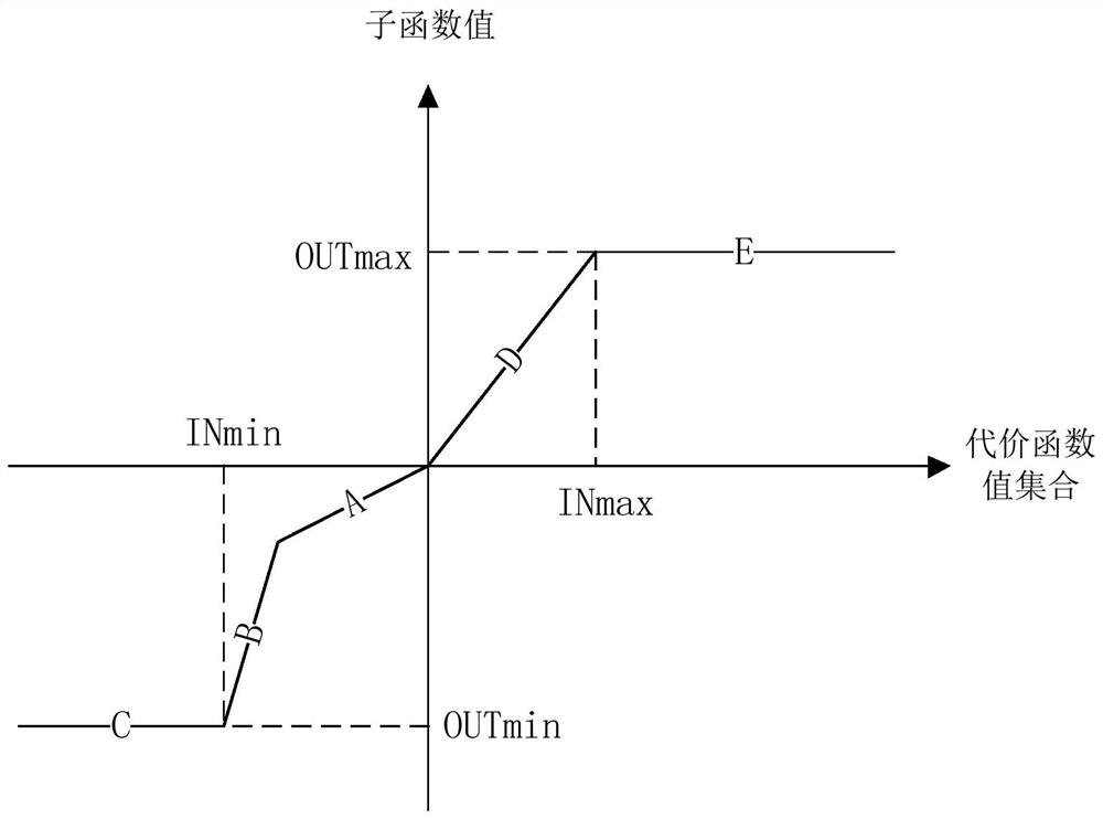
[0034] The cost function value set corresponding to at least one parameter to be optimized includes several sub-costs, and each sub-cost is the value of the parameter to be optimized corresponding to each category obtained by dividing the FPGA chip according to a predetermined classi...


PUM


Abstract

The invention discloses a novel FPGA chip layout optimization method, which relates to the technical field of FPGAs. The method comprises the following steps of: processing and mapping a cost functionvalue set corresponding to at least one parameter to be optimized by using a corresponding filtering function, and taking a processed result as a sub-function value, wherein at least one cost function value set comprises sub-costs corresponding to a plurality of categories; then performing weighted addition on each sub-function value according to the respective corresponding weight to obtain an objective function value for layout optimization. According to the method, the debugging method of the influence on each to-be-optimized parameter in the objective function is changed in the iterativeprocess, the filtering function corresponding to each cost function value set is utilized to perform corresponding mapping processing on each sub-cost in the cost function value set, not only a singleweight value is utilized to perform adjustment, the filtering function has diversity, different sub-costs can be mapped respectively, the debugging process is more flexible, and the adaptability andthe pertinence are higher.

Description

technical field [0001] The invention relates to the field of FPGA technology, in particular to a novel FPGA chip layout optimization method. Background technique [0002] Field-Programmable Gate Array (Field-Programmable Gate Array, FPGA) is a chip widely used in household appliances, large machinery and even aerospace. With the expansion of the scale of FPGA chips, the layout of the chip is becoming more and more critical and important, which directly affects the performance of the chip area, frequency and so on. Therefore, it is necessary to comprehensively consider the cost of various aspects in the chip layout. Under the condition of satisfying various constraints, how to optimize the chip layout to ensure the performance and distributability of the chip becomes the key to ensure the quality of the chip. [0003] At present, the planning problem will be introduced into the layout optimization of FPGA, and the layout optimization objective function of FPGA planning probl...

Claims


Application Information

Patent Timeline
IPC IPC(8): G06F30/392
CPCG06F30/392
Inventor 虞健周洋洋董志丹王新晨刘佩季振凯
Owner WUXI ESIONTECH CO LTD
Why Eureka
Try Eureka