
Chip processing material receiving and feeding device

A chip and material receiving box technology, applied in the direction of conveyor objects, transportation and packaging, electrical components, etc., can solve the problems of chip placement disorder and low work efficiency, and achieve convenient processing operations, high practicability, and unified location Effect

Inactive Publication Date: 2021-01-19
合肥高地创意科技有限公司
View PDF0 Cites 1 Cited by
  • Summary
  • Abstract
  • Description
  • Claims
  • Application Information

AI Technical Summary

Problems solved by technology

[0002] The chip is the core component of the reorganization circuit, and it is also the base point for programming numerical control data storage and receiving. Wires and pins achieve the wiring processing effect, and the chip needs to be picked up and fed during the processing process. The existing chip feeding device automatically feeds the chip, and the position of the chip is relatively disordered. Subsequent processing also requires manual finishing, resulting in low work efficiency

Method used


Image

  • Chip processing material receiving and feeding device
  • Chip processing material receiving and feeding device
  • Chip processing material receiving and feeding device

Examples


Embodiment Construction

[0022] In order to make the object, technical solution and advantages of the present invention clearer, the present invention will be further described in detail below in conjunction with the accompanying drawings and embodiments. It should be understood that the specific embodiments described here are only used to explain the present invention, not to limit the present invention.

[0023] The components of the embodiments of the invention generally described and shown in the figures herein may be arranged and designed in a variety of different configurations. Accordingly, the following detailed description of the embodiments of the invention provided in the accompanying drawings is not intended to limit the scope of the claimed invention, but merely represents selected embodiments of the invention.

[0024] Based on the embodiments of the present invention, all other embodiments obtained by persons of ordinary skill in the art without making creative efforts belong to the pro...


PUM


Abstract

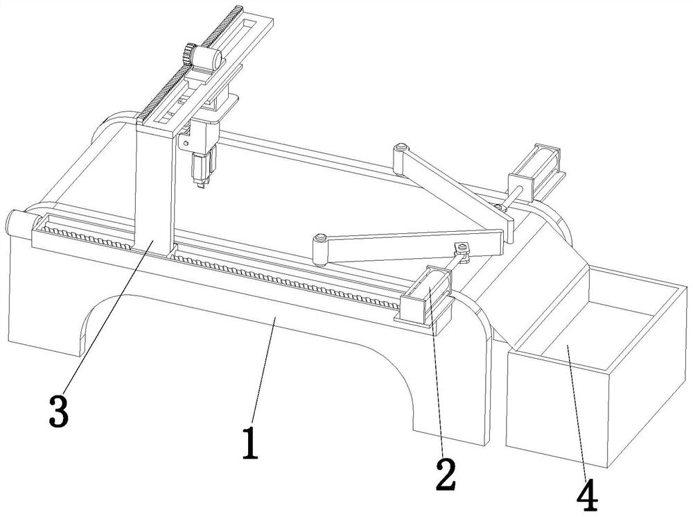
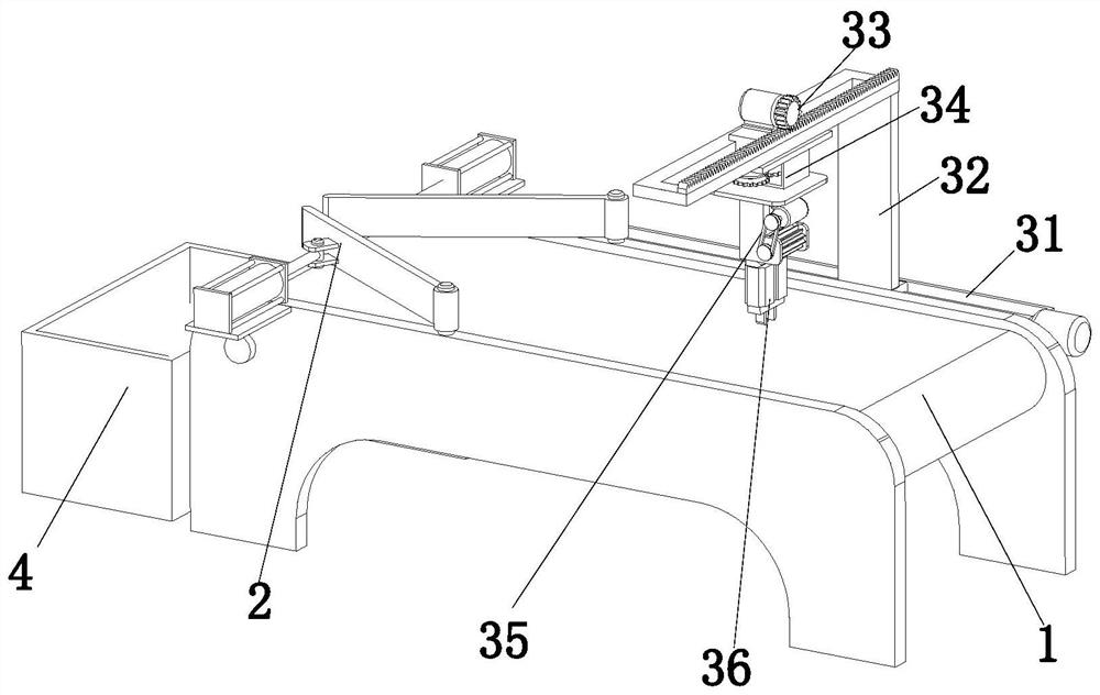
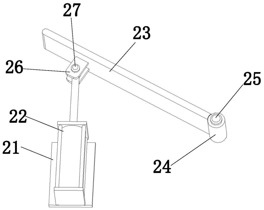
The invention discloses a chip processing material receiving and feeding device, and relates to the technical field of chip processing. The device comprises a feeding conveying table, two groups of guide mechanisms, a stacking mechanism and a material receiving mechanism, wherein the two groups of guide mechanisms are the same in structure, and the two groups of guide mechanisms are symmetricallyarranged on two sides of the feeding conveying table; the stacking mechanism is arranged on one side of the feeding conveying table and comprises a moving assembly, a mounting rod, a position adjusting assembly, a steering adjusting assembly, a lifting adjusting assembly and a mechanical clamping jaw, and the material receiving structure is arranged at the conveying end of the feeding conveying table. According to the chip feeding device, automatic arrangement of the positions in chip machining is completed through cooperative work of all the mechanism assemblies, so the positions of chips during feeding can be unified, manual arrangement is not needed, subsequent machining operation is facilitated, and the practicability is high.

Description

technical field [0001] The invention relates to the technical field of chip processing, in particular to a chip processing receiving and feeding device. Background technique [0002] The chip is the core component of the reorganization circuit, and it is also the base point for programming numerical control data storage and receiving. Wires and pins achieve the wiring processing effect, and the chip needs to be picked up and fed during the processing process. The existing chip feeding device automatically feeds the chip, and the position of the chip is relatively disordered. Subsequent processing also requires manual finishing, resulting in low work efficiency. Contents of the invention [0003] The object of the present invention is to provide a chip processing pick-up and feed device to solve the technical problems mentioned in the background art. [0004] The invention provides a pick-up and delivery device for chip processing, which includes a feeding and conveying p...

Claims


Application Information

Patent Timeline
Patent Type & Authority Applications(China)
IPC IPC(8): H01L21/67H01L21/677
CPCH01L21/67271H01L21/67706H01L21/67721
Inventor 陈圆圆
Owner 合肥高地创意科技有限公司
Learn More