[0012]The present invention will be described in further detail below in conjunction with the accompanying drawings.
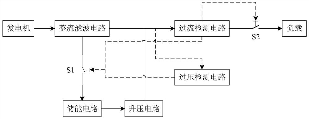
[0013]The overflow energy storage type power supply circuit of the present invention is adapted to a micro generator and includes an energy storage circuit, a rectifier filter circuit, a booster circuit, an overvoltage detection circuit, an overcurrent detection circuit, and a first switch control circuit S1 and the second switch control circuit S2.
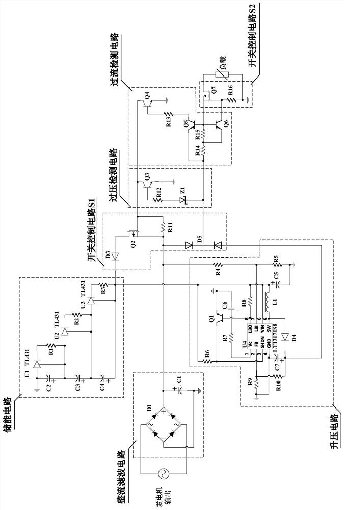
[0014]Such asfigure 1 As shown, the solid line represents the connection between the main circuits, and the dotted line represents the connection between the control circuits. In the main circuit, the output terminal of the generator is connected to the input terminal of the rectifier filter circuit. The output terminal of the rectifier filter circuit is divided into two channels, one is directly connected to the input terminal of the overcurrent detection circuit, and the other one passes through the first switch control circuit in turn S1, the tank circuit, and the boost circuit are connected to the input end of the overcurrent detection circuit, and the output end of the overcurrent detection circuit is connected to the load through the second switch control circuit S2. In the control circuit, the input terminal of the overvoltage detection circuit is connected with the input terminal of the overcurrent detection circuit, the output terminal of the overvoltage detection circuit is connected with the control terminal of the first switch control circuit S1, and the output terminal of the overcurrent detection circuit is connected with the first switch control circuit S1. The control terminals of a switch control circuit S1 and a second switch control circuit S2 are connected.
[0015]Among them, the energy storage circuit can be used to store the excess electrical energy when the generator speed is high or overload; the use of the boost circuit can be used to increase the previously stored electrical energy when the generator speed is low or stop rotating. The voltage is required to extend the power supply time of the generator and improve efficiency; the over-current detection circuit can cut off the load when overloaded, and store the electrical energy in the energy storage circuit for subsequent use.
[0016]Such asfigure 2As shown, the circuit structures and principles of the above-mentioned tank circuit, rectifier filter circuit, boost circuit, overvoltage detection circuit, overcurrent detection circuit, first switch control circuit S1, and second switch control circuit S2 are described in sequence below:
[0017]The tank circuit includes a second capacitor C2, a third capacitor C3, a fourth capacitor C4, a first reference source U1, a second reference source U2, a third reference source U3, a first resistor R1, a second resistor R2, and a Three resistors R3. The negative pole of the second capacitor C2 and the anode of the first reference source U1 are respectively grounded, the positive pole of the second capacitor C2 is divided into two paths, one is connected to the reference pin of the first reference source U1, and the other is connected to the negative electrode of the third capacitor C3. One end of the first resistor R1 is connected to the cathode of the first reference source U1, and the other end is respectively connected to the reference pin of the first reference source U1 and the anode of the second reference source U2. The anode of the third capacitor C3 is divided into two ways, and one way is connected The reference pin of the second reference source U2, the other is connected to the negative electrode of the fourth capacitor C4, one end of the second resistor R2 is connected to the cathode of the second reference source U2, and the other end is connected to the reference pin of the second reference source U2 and the The anode of the three reference sources U3, the anode of the fourth capacitor C4 is connected to the reference pin of the third reference source U3, one end of the third resistor R3 is connected to the cathode of the third reference source U3, and the other end is divided into three ways, the first way is connected The reference pin of the third reference source U3, the second path is connected to the boost circuit, and the third path is connected to the first switch control circuit S1.
[0018]In the energy storage circuit, the three capacitors are all Farad capacitors, and the models of the three reference sources are all TL431. The withstand voltage of the tank circuit obtained by connecting three farad capacitors in series is much higher than that of a single farad capacitor, and when the charging voltage is higher than the reference voltage value inside the TL431, the transistor of the output stage is turned on, and the farad capacitor is supported by the TL431 Circuit leakage to ensure that the voltage across the farad capacitor will not exceed its own withstand voltage.
[0019]The rectifying and filtering circuit includes a first rectifying bridge D1 and a first capacitor C1. The output terminal of the generator is connected to the AC input terminal of the first rectifier bridge D1, and the DC output terminal of the first rectifier bridge D1 is connected in parallel with the first capacitor C1. The negative electrode of the first capacitor C1 is grounded, and the positive electrode of the first capacitor C1 is connected to The booster circuit is connected to the first switch control circuit S1.
[0020]In the rectifying and filtering circuit, the sinusoidal voltage output by the generator is rectified and filtered to obtain a pulsating DC voltage.
[0021]The boost circuit includes a fourth power management chip U4, a fourth diode D4, a first transistor Q1, a first inductor L1, a fifth capacitor C5, a sixth capacitor C6, a seventh capacitor C7, and a fourth resistor. R4, fifth resistor R5, sixth resistor R6, seventh resistor R7, eighth resistor R8, ninth resistor R9, and tenth resistor R10. The compensation pin Vc of the fourth power management chip U4 is grounded through the seventh resistor R7 and the sixth capacitor C6 in turn, the feedback pin FB of the fourth power management chip U4 is grounded through the ninth resistor R9, and one end of the tenth resistor R10 is connected to the The feedback pin FB of the four power management chip U4, the other end is divided into three ways, the first way is connected to the anode of the seventh capacitor C7, the second way is connected to the cathode of the fourth diode D4, and the third way is connected to the first switch In the control circuit S1, the shutdown pin SHDN of the fourth power management chip U4 is connected to one end of the sixth resistor R6 and the collector of the first transistor Q1, the emitter of the first transistor Q1 is grounded, and the first transistor is grounded. The base of Q1 is respectively connected to the undervoltage output pin LBO of the fourth power management chip U4 and one end of the eighth resistor R8. The ground pin GND of the fourth power management chip U4 is connected to the cathode of the seventh capacitor C7, and the fourth power management The ground pin GND of the chip U4 is connected to ground, and the switch pin SW of the fourth power management chip U4 is divided into two paths, one is connected to the anode of the fourth diode D4, and the other is connected to one end of the first inductor L1, the first inductor The other end of L1 is connected to the positive pole of the fifth capacitor C5, the voltage input pin VIN of the fourth power management chip U4, the other end of the eighth resistor R8, the other end of the sixth resistor R6, and the tank circuit, and the fifth capacitor C5 The negative pole of and one end of the fifth resistor R5 are grounded respectively. The other end of the fifth resistor R5 is divided into two paths, one is connected to the undervoltage input pin LBI of the fourth power management chip U4, and the other is connected to one end of the fourth resistor R4. The other end of the fourth resistor R4 is divided into two ways, one way is connected to the positive electrode of the first capacitor C1 in the rectifying and filtering circuit, and the other way is connected to the first switch control circuit S1.
[0022]In the boost circuit, the model of the power management chip is LT1317, the chip is embedded with a switch tube, the switch tube and the first inductor L1, the fourth diode D4, the fifth capacitor C5, and the seventh capacitor C7 form a Boost circuit . The ninth resistor R9 and the tenth resistor R10 are voltage sampling elements in the feedback loop, and their ratio determines the output voltage of the boost circuit. The seventh resistor R7 and the sixth capacitor C6 compensate the internal error amplifier of the chip to improve its frequency response characteristics. The fourth resistor R4 and the fifth resistor R5 are sampling elements for the DC voltage obtained after filtering. When the filtered voltage is greater than the required output voltage, the undervoltage output pin outputs a low level, the first transistor Q1 is turned off, and the power management The boost function of the chip is turned off. When the filtered voltage is less than the required output voltage, the under-voltage output pin outputs a high level, the first transistor Q1 is turned on, the boost function of the power management chip is turned on, and the boost circuit starts Work to increase the voltage in the tank circuit to the required voltage. In addition, the sixth resistor R6 and the eighth resistor R8 are used as pull-up resistors.
[0023]The overvoltage detection circuit includes a third transistor Q3, a first voltage regulator Z1 and a twelfth resistor R12. The cathode of the first voltage regulator tube Z1 is divided into two paths, the first path is connected to the first switch control circuit S1, the second path is connected to the overcurrent detection circuit, and the anode of the first voltage regulator tube Z1 is connected to the third through the twelfth resistor R12. The base of the triode Q3, the emitter of the third triode Q3 are grounded, and the collector of the third triode Q3 is connected to the first switch control circuit S1.
[0024]In the overvoltage detection circuit, when the input voltage exceeds the turn-on voltage of the first Zener tube Z1, the third transistor Q3 is turned on and outputs a low-level overvoltage control signal to the first switch control circuit S1.
[0025]The overcurrent detection circuit includes a fourth transistor Q4, a fifth transistor Q5, a sixth transistor Q6, a thirteenth resistor R13, a fourteenth resistor R14, and a fifteenth resistor R15. The emitter of the fifth transistor Q5 is connected to one end of the fourteenth resistor R14 and the cathode of the first voltage regulator Z1 in the overvoltage detection circuit, and the other end of the fourteenth resistor R14 is divided into two ways, all the way to the The emitter of the hexatransistor Q6, the other is connected to one end of the fifteenth resistor R15, and the other end of the fifteenth resistor R15 is divided into three ways, of which the first is connected to the switch control circuit S2, and the second is connected to the fifth and third The base of the transistor Q5, the third way is connected to the base of the sixth transistor Q6, the collector of the sixth transistor Q6 is connected to the switch control circuit S2, and the collector of the fifth transistor Q5 passes through the thirteenth resistor R13 is connected to the base of the fourth triode Q4, the emitter of the fourth triode Q4 is grounded, and the collector of the fourth triode Q4 is connected to the collector of the third triode Q3 in the overvoltage detection circuit.
[0026]In the overcurrent detection circuit, as the output current increases, the voltage across the fourteenth resistor R14 and the fifteenth resistor R15 as the current sampling resistor increases, and the fifth transistor Q5 and the sixth transistor Q6 turns on one after another. After the fifth transistor Q5 is turned on, the fourth transistor Q4 is also turned on, and outputs a low-level overcurrent control signal to the first switch control circuit S1; after the sixth transistor Q6 is turned on, its The voltage between the emitter and the collector becomes very small, and a high-level overcurrent control signal is output to the second switch control circuit S2.
[0027]The first switch control circuit S1 includes a second MOS transistor Q2, a third diode D3, an eleventh resistor R11, and a fifth common cathode diode D5. The cathode of the third diode D3 is respectively connected to the third resistor R3 in the tank circuit and the sixth resistor R6 in the boost circuit. The anode of the third diode D3 is connected to the drain of the second MOS transistor Q2, and the second MOS transistor The gate of Q2 is connected to one end of the eleventh resistor R11 and the collector of the third transistor Q3 in the overvoltage detection circuit, and the source of the second MOS transistor Q2 is connected to the other end of the eleventh resistor R11 and the fifth One anode of the common cathode diode D5, the other anode of the fifth common cathode diode D5 is connected to the anode of the seventh capacitor C7 in the boost circuit, and the cathode of the fifth common cathode diode D5 is connected to the first voltage regulator Z1 in the overvoltage detection circuit The cathode.
[0028]In the first switch control circuit S1, when the DC voltage obtained after rectification and filtering is relatively high, the upper tube of the fifth common cathode diode D5 is turned on, the lower tube is turned off, and the rectified and filtered electric energy is directly sent to the load through the upper tube When the voltage on the filter capacitor drops, the lower tube of the fifth common cathode diode D5 is turned on, and the upper tube is turned off. The energy in the tank circuit is boosted by the booster circuit and then sent to the load to ensure that the load is in the entire The power supply voltage obtained during the working time is kept within a proper range; when the input voltage is too high or the output current is too large, the gate of the second MOS transistor Q2 is pulled to a low level, and current flows across the eleventh resistor R11 However, when the voltage across the eleventh resistor R11 is greater than the turn-on threshold of the MOS transistor, the second MOS transistor Q2 is turned on, and the rectified and filtered electric energy is sent to the energy storage circuit to store the excess electric energy.
[0029]The second switch control circuit S2 includes a seventh MOS transistor Q7 and a sixteenth resistor R16. The source of the seventh MOS transistor is connected to the base of the fifth transistor Q5 in the overcurrent detection circuit, and the gate of the seventh MOS transistor is divided into two ways, one way is connected to the sixth transistor Q6 in the overcurrent detection circuit. The collector is connected, the other is grounded through the sixteenth resistor R16, and the load is connected in parallel between the drain of the seventh MOS transistor and ground.
[0030]In the second switch control circuit S2, when the output current is too large, the gate potential of the seventh MOS transistor Q7 is raised to be equivalent to the source, and the seventh MOS transistor Q7 is turned off to disconnect the load from the main circuit .
[0031]In the previous stage of generator operation (the speed is higher at this time), the electric energy gets a higher DC voltage after the rectifier filter circuit, the boost circuit does not work, the overvoltage detection circuit outputs a control signal to turn on the second MOS transistor Q2 At this time, part of the electric energy is sent to the load through the flow detection circuit and the seventh MOS tube Q7 in turn, and the other part of the electric energy is sent to the energy storage circuit through the second MOS tube Q2; and in the latter stage of the power generation device (the speed is lower at this time) Or has stopped rotating), the DC voltage obtained after rectification and filtering is lower, the boost circuit works, and under its action, the electric energy in the tank circuit is raised to the required voltage, and the overvoltage detection circuit outputs a control signal to make the second The MOS transistor Q2 is turned off, and the electric energy is sent to the load through the energy storage circuit, the boost circuit, the overcurrent detection circuit and the seventh MOS transistor Q7 in turn; in addition, when the load is overcurrent or short-circuited, the overcurrent detection circuit outputs a control signal to make the second The MOS transistor Q2 is turned on, the seventh MOS transistor Q7 is turned off, the load is disconnected from the main circuit, and all electrical energy is sent to the energy storage circuit.