Memory and method of forming the same

A memory and bit line technology, applied in the manufacturing of semiconductor devices, electrical solid state devices, semiconductor/solid state devices, etc., can solve problems such as large parasitic effects of memory, reduce dielectric constant, increase top surface contact area, and improve parasitic effects Effect

Active Publication Date: 2022-02-08
FUJIAN JINHUA INTEGRATED CIRCUIT CO LTD
View PDF3 Cites 0 Cited by
  • Summary
  • Abstract
  • Description
  • Claims
  • Application Information

AI Technical Summary

Problems solved by technology

[0004] The purpose of the present invention is to provide a memory to solve the problem of large parasitic effects in the existing memory

Method used


Image

  • Memory and method of forming the same
  • Memory and method of forming the same
  • Memory and method of forming the same

Examples


Embodiment Construction
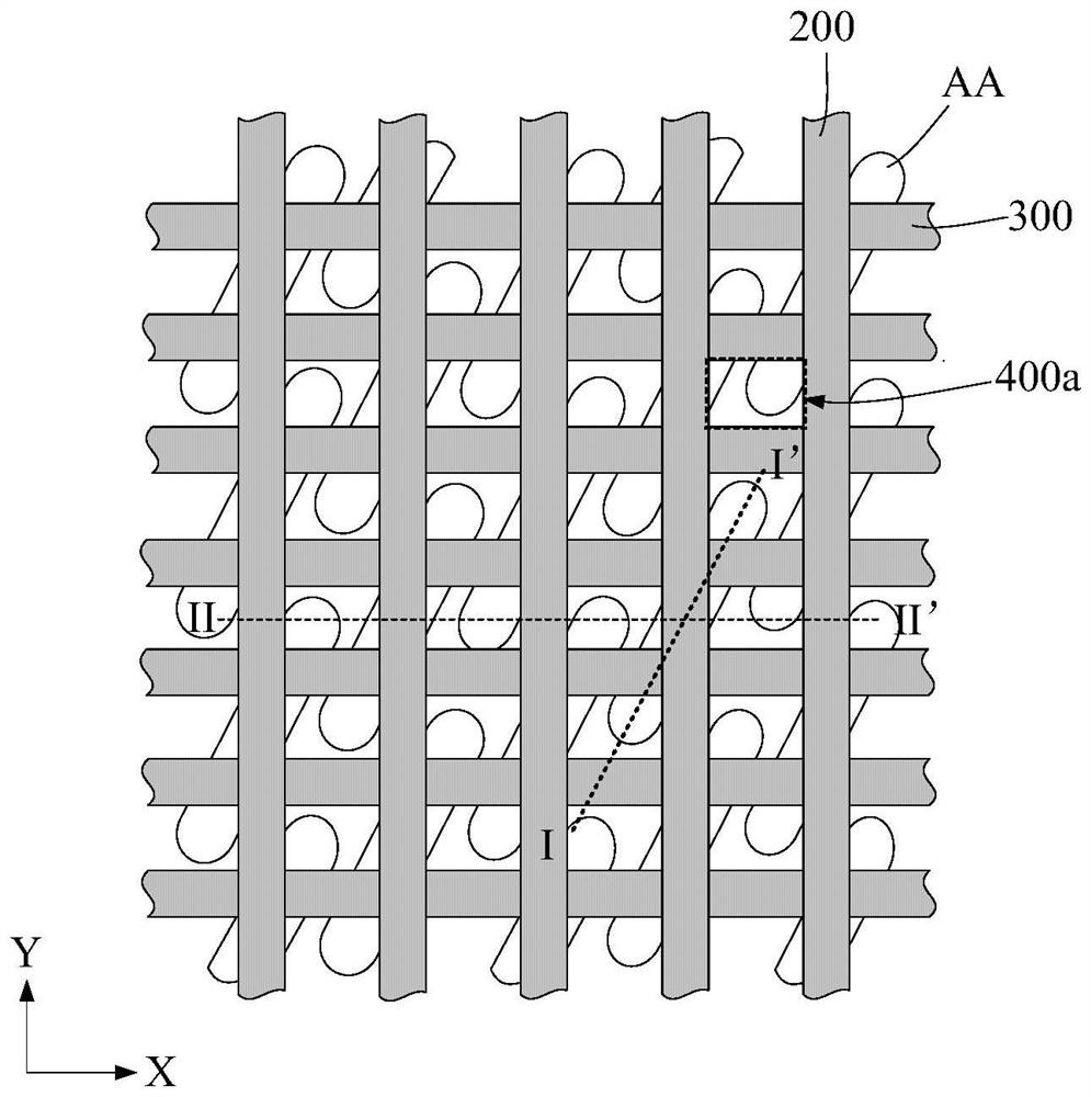
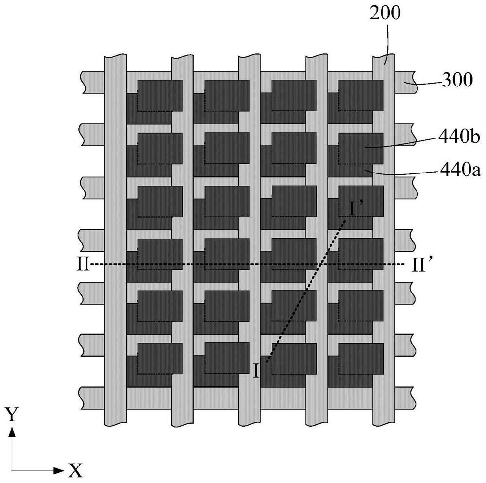
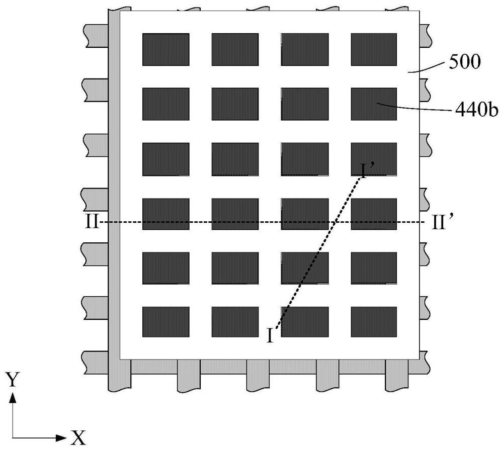
[0073] The core idea of ​​the present invention is to provide a memory, including a substrate, and a plurality of bit lines and a plurality of insulating lines formed on the substrate. Wherein, the intersection of the bit line and the insulating line defines a plurality of node contact windows on the substrate, and the node contact windows are filled with contact plugs. Further, a spacer structure is also formed between the tops of adjacent contact plugs, and gaps are formed in the spacer structures, so as to reduce the dielectric constant of the spacer structures, thereby improving the distance between adjacent contact plugs. parasitic effects between them.

[0074] The memory and its forming method proposed by the present invention will be further described in detail below with reference to the drawings and specific embodiments. The advantages and features of the present invention will become clearer from the following description. It should be noted that all the drawings ...


PUM


Abstract

The invention provides a memory and its forming method. A node contact window is defined by a bit line and an insulating line, and the contact plug filled in the node contact window also protrudes upward from the node contact window, and a spacer structure is further used to space adjacent contact plugs, and the spacer structure The first gap is also formed in the contact plug, which is beneficial to reduce the dielectric constant of the dielectric material between the adjacent contact plugs, and effectively improve the parasitic effect of the device.

Description

technical field [0001] The invention relates to the technical field of semiconductors, in particular to a memory and a forming method thereof. Background technique [0002] With the development of semiconductor technology, the density of semiconductor elements in integrated circuits has increased, and the spacing between adjacent semiconductor elements has also decreased, resulting in the parasitic effects between adjacent conductive parts becoming more and more incompatible. ignore. [0003] Specifically, for a dynamic random access memory (Dynamic Random Access Memory, DRAM), it usually has a storage cell array, the storage cell array includes a plurality of storage cells arranged in an array, and the memory also has multiple Each bit line is electrically connected to a corresponding memory cell, and the memory also includes a storage capacitor for storing charge representing stored information, and the memory cell can be inserted through a contact The storage capacitors...

Claims


Application Information

Patent Timeline
Patent Type & Authority Patents(China)
IPC IPC(8): H01L27/108H01L21/8242H01L21/768
CPCH01L21/76897H10B12/30H10B12/485
Inventor 陈肯利陈琮文
Owner FUJIAN JINHUA INTEGRATED CIRCUIT CO LTD
Why Eureka
Try Eureka