Capping layer for extreme low dielectric constant films

Inactive Publication Date: 2005-04-05
APPLIED MATERIALS INC
View PDF56 Cites 114 Cited by
  • Summary
  • Abstract
  • Description
  • Claims
  • Application Information

AI Technical Summary

Benefits of technology

[0014]Embodiments of the present invention provide a silicon-carbide-type or silicon oxycarbide (also often called carbon-doped-oxide [CDO] or organosilicate glass) capping material and method for depositing this capping material on ELK films which are used as a dielectric material in integrated circuits. The ELK film may include any ELK film including but not limited to inorganic, organic and hybrid dielectric materials and their respective porous versions. The capping material may be an amorphous, hydrogenated silicon carbide type material such as the commercially available BLOk™ material, or a carbon-doped oxide material such as the commercially available Black Diamond™ both of which are developed by Applied Materials of Santa Clara, Calif. The amorphous silicon carbide (a-SiC) material is, deposited using a plasma process in a non-oxidizing environment and the CDO-type ma

Problems solved by technology

In terms of deposition techniques, both spin-on and chemical vapor deposition (“CVD”) processes are under development, with key challenges remaining around issues of technological performance—i.e. integration.
However, copper has its own difficulties for IC manufacturing processes.
However, as explained above, with the smaller feature sizes and increased diffusion propensity of copper, the prior barrier layers are inadequate for optimal performance.
Such integration methods when using ELK material and especially porous dielectric materials place additional demands upon the liner or barrier layers.
High dielectric constants result in a capped insulator layer that does not significantly reduce the overall dielectric constant for the combined insulator-capping layer, which defeats the goals of reducing the dielectric constant of the insulating material.
Similarly, problems remain in depositing a silicon dioxide capping layer on a porous film.
Such an oxidative process damages the surface functionality of the

Method used


Image

  • Capping layer for extreme low dielectric constant films
  • Capping layer for extreme low dielectric constant films
  • Capping layer for extreme low dielectric constant films

Examples


Embodiment Construction

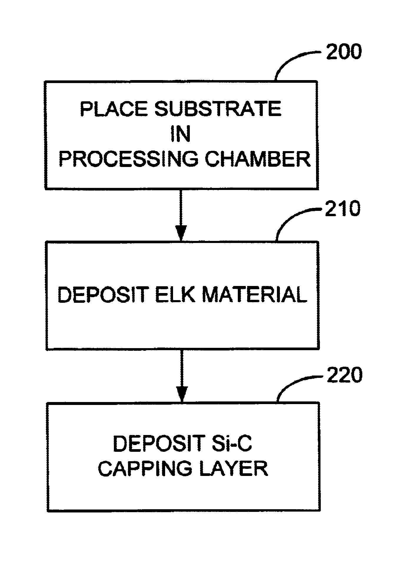
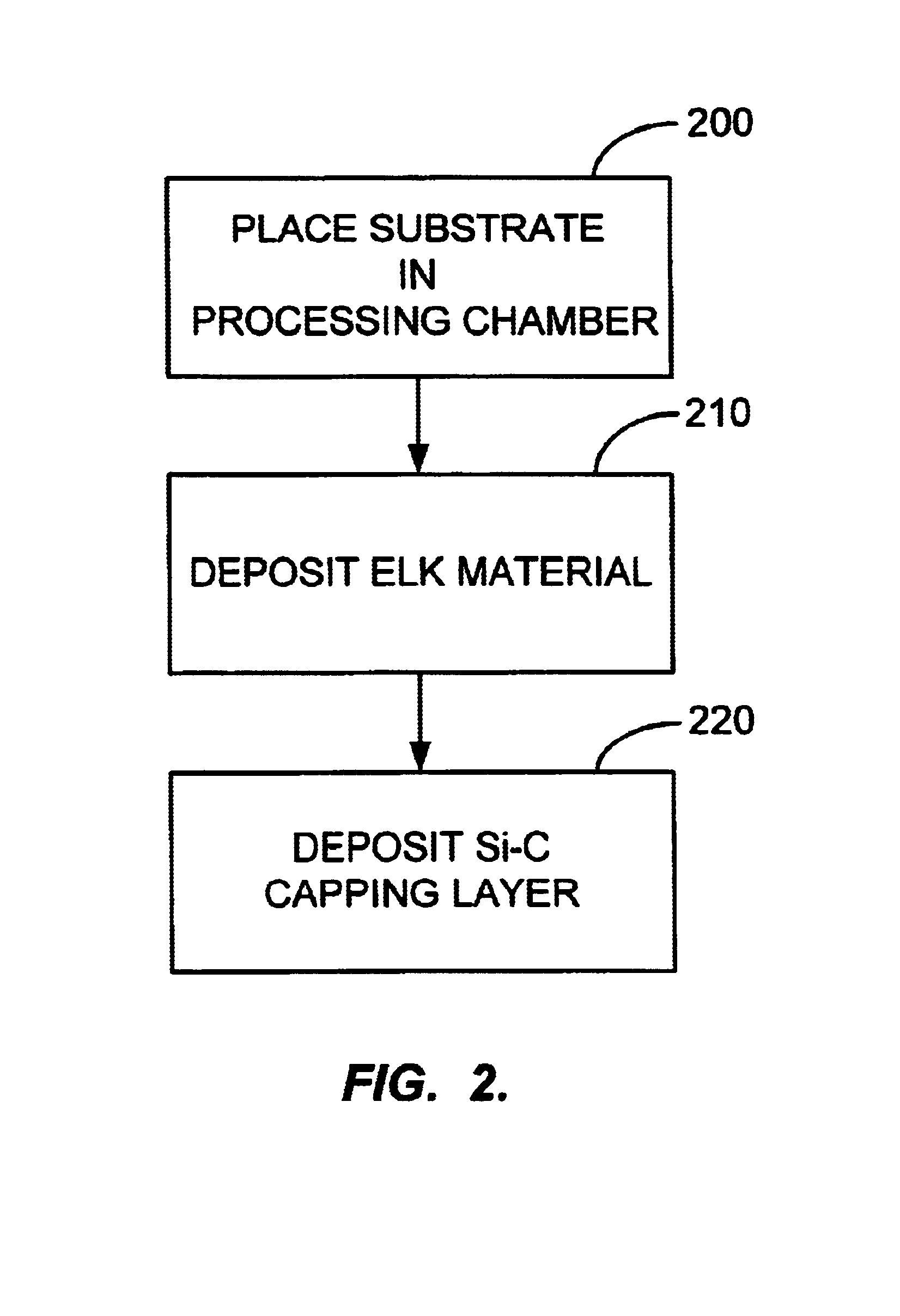
[0019]Embodiments of this invention provide a method to deposit a silicon carbide type low dielectric constant film as a capping layer or a carbon doped silicon oxide film as a capping layer or a combination thereof over an extremely low dielectric constant (“ELK”) film that may contain oxidizable Si—CH3 and / or Si—H groups. The capping layer is deposited using a PECVD process in either a non-oxidizing or an oxygen starved plasma. Both the non-oxidizing and the oxygen starved plasma processes prevent or minimize oxidation of the underlying ELK film.

[0020]The lack of an oxidizing plasma in the PECVD deposition process allows the capping layer to be deposited without degrading the ELK film. Using process conditions described below capping layers having a dielectric constant below 5 and preferably below 3 is deposited on an ELK film. Using these process conditions, the deposition regime of the capping layer does not oxidize the Si—CH3 or Si—H bonds in the ELK film, and thus allows for a...


PUM

PropertyMeasurementUnit
Temperatureaaaaaaaaaa
Lengthaaaaaaaaaa
Pressureaaaaaaaaaa

Abstract

Specific embodiments of the invention provide a silicon-carbide-type or silicon oxycarbide (also often called carbon-doped-oxide [CDO] or organosilicate glass) capping material and method for depositing this capping material on ELK films which are used as a dielectric material in integrated circuits. The ELK film may include any ELK film including but not limited to inorganic, organic and hybrid dielectric materials and their respective porous versions. The silicon-carbide-type material may be an amorphous silicon carbide type material such as the commercially available BLOk™ material, or a carbon-doped oxide material such as the commercially available Black Diamond™ both of which are developed by Applied Materials of Santa Clara, Calif. The amorphous silicon carbide (a-SiC) material is deposited using a plasma process in a non-oxidizing environment and the CDO-type material is deposited using an oxygen-starved plasma process. The non-oxidative or oxygen-starved plasma processes do not significantly degrade the underlying film's chemical and electrical properties. The CDO material offers the advantageous property of having a lower dielectric constant value of less than 3.5 as opposed to the a-SiC material which has a dielectric constant of approximately 4.5. The CDO material besides, having a lower dielectric constant also has a superior adhesion characteristics to the underlying ELK material. However, experiments have indicated that despite its higher dielectric constant, the a-SiC-type material (e.g. BLOk™) may be used to generate capped ELK films with similar or even reduced dielectric constants relative to lower k capped films, and may provide composite (i.e. ELK+cap) structures exhibiting superior k stability.

Description

CROSS-REFERENCES TO RELATED APPLICATIONS[0002]This application claims the benefit of U.S. Provisional Application Ser. No. 60 / 160,050, filed Oct. 18, 1999, which is incorporated herein by reference.BACKGROUND OF THE INVENTION[0003]The present invention relates to the formation of dielectric layers. More particularly, embodiments of the present invention relate to a method for capping a low dielectric constant film that is particularly useful as a premetal or intermetal dielectric layer in an integrated circuit.[0004]Semiconductor device geometries have dramatically decreased in size since integrated circuits were first introduced several decades ago, and all indications are that this trend will continue. Today's wafer fabrication plants are routinely producing devices having 0.25 μm and even 0.18 μm feature sizes, and the plants of the future will soon be producing devices having even smaller geometries.[0005]The drive to faster and faster microprocessors, and more powerful microele...

Claims


Application Information

Patent Timeline
IPC IPC(8): C23C16/32H01L21/70H01L21/02H01L21/768H01L21/314H01L21/316H01L21/312
CPCC23C16/325H01L21/02167H01L21/022H01L21/02203H01L21/02211H01L21/02274H01L21/02282H01L21/312H01L21/3148H01L21/31633H01L21/76828H01L21/76829H01L21/02126Y10S438/97H01L21/76807
Inventor WEIDMAN, TIMOTHYNAULT, MICHAEL PCHANG, JOSEPHINE J
Owner APPLIED MATERIALS INC
Why Eureka
Try Eureka