Method of forming low-k dielectrics

a dielectric and low-k technology, applied in the field of thin films, can solve the problems of reliability failure, increased softness, brittleness and cracking, and high cost of increased softness, and achieves rapid thermal curing, improved dielectric constant performance, and excellent mechanical and thermal properties

Inactive Publication Date: 2005-03-24
SILECS OY
View PDF7 Cites 111 Cited by
  • Summary
  • Abstract
  • Description
  • Claims
  • Application Information

AI Technical Summary

Benefits of technology

It is an aim of the present invention to eliminate the disadvantages of the prior art and to improve the dielectric constant performance of known organic, inorganic and organic-inorganic materials through rapid thermal curing and to provide novel low dielectric constant thin films, which have excellent mechanical and thermal properties.
It is a fourth object of the invention to have achieve a rapid curing process, which allows the control the micro porosity of the material and furthermore tunability of dielectric constant of the thin film by adjusting dT, i.e., the difference between minimum and maximum temperature in the rapid curing process.
Considerable advantages are achieved by the invention. Thus, when using a nonporous dielectric starting material, nonporous materials having a porosity volume of less than 30% and a pore radius of approximately 1 nm or less, can be produced. These materials have a relative dielectric constant of less than 2.6 and high elasticity (Young's modulus 4 GPa or higher). The process is faster than the present day processes, cutting processing times to one sixth or less.

Problems solved by technology

Silicate-based low-k materials can demonstrate exceptional thermal stability and usable modulus but can be plagued by brittleness and cracking.
Organic materials, by contrast, often show improved material toughness, but at the expense of increased softness, lower thermal stability, and higher thermal expansion coefficients.
Porous materials sacrifice mechanical properties and possess a strong tendency of absorbing chemicals used in semiconductor fabrication leading to reliability failures.
Fluorinated materials can induce corrosion of metal interconnects, rendering a chip inoperative.
Generally, in low-k materials, mechanical robustness and thermal conductivity has been sacrificed as compared to their pure silicon dioxide analogues, making integration into the fabrication flow very challenging.
Further, known materials comprising exclusively inorganic bonds making up the siloxane matrix are brittle and have poor elasticity at high temperatures.
However, in spite of advantages achieved by using the known precursors, there are still disadvantages of the known methods of their manufacture.
First, the manufacture of these precursors is inefficient because the chemical reactions have low yields, and the processes are expensive and produce toxic byproducts.
Further, it is difficult to eliminate redimerization of the reactive intermediates.
When deposited along with polymers, these dimers decrease the thermal stability and mechanical strength of the film.
Moreover, materials currently reaching a dielectric constant of less than 2.5 are typically highly porous, which makes the integration of such materials into the semiconductor device very difficult.
Thus, the prior art contains no examples of ways of processing dielectric material precursors for semiconductor manufacture to provide dielectric materials, which have desired properties of low dielectric constant with low controlled micro porosity, high thermal stability, and low cost.

Method used


Image

  • Method of forming low-k dielectrics
  • Method of forming low-k dielectrics
  • Method of forming low-k dielectrics

Examples


examples

Synthesis of Molecules

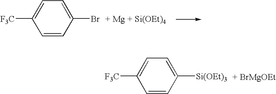
(#1) 4-(trifluoromethyl)phenyl trichlorosilane, 4-(F3C)C6H4SiCl3

Preparation:

96.24 g (0.427 mol) 4-(trifluoromethyl)phenyl bromide, 10.38 g (0.427 mol) magnesium, and a small amount of iodine are stirred for half an hour. 356.78 g (382 ml, 1.708 mol) Si(OEt)4 is added to solution. Et2O is added until exothermic reaction occurs (˜200 ml) and the solution is refluxed for over night. Et2O is evaporated off and 250 ml n-heptane is added. Mg-salts are filtered off. n-heptane is evaporated and remaining 4-(F3C)C6H4Si(OEt)3 is purified by distillation. B.p. 68° C. / 1 mbar. Yield 50.22 g (38%).

50.22 g (0.163 mol) 4-(trifluoromethyl)phenyl triethoxysilane, 83 mL (1.140 mol, 135.62 g) thionylchloride and 2.45 g (0.021 mol) pyridinium hydrochloride were refluxed and stirred for 16 h. Excess of SOCl2 was evaporated and residue was fractionally distilled to obtain 37 g (81%) 4-(trifluoromethyl)phenyl trichlorosilane. B.p. 44° C. / 4.0 mbar.

Characterization:

4-(trifl...

example a

Vinyl trichlorosilane (0.05 mol), 4-trifluoromethyl phenyl trichlorosilane (0.45 mol) and methyl trichlorosilane (0.55 mol) are dissolved in dehydrated DCM (800 ml). The solution is added drop-wise into a flask containing excess of water (45 mol) while stirring the solution.

After addition of the water, the solution stirred for 1 hour at the room temperature. The solution is neutralized by water extraction for 12 times and finally volatile components are evaporated with rotary evaporator. After vacuum treatment, dehydrated 400 w-% of mesitylene used as process solvent is added into the material and the material is carefully homogenized. Appropriate initiators are added and dissolved into the mixture. Finally the material is filtered.

example b

Vinyl trichlorosilane (0.05 mol), adamantyltrichlorosilane (0.57 mol) and methyl trichlorosilane (0.38 mol) are dissolved in dehydrated DCM (800 ml). The solution is added drop-wise into a flask containing excess of water (45 mol) while stirring the solution. After addition of the water, the solution stirred for 1 hour at the room temperature. The solution is neutralized by water extraction for 12 times and finally volatile components are evaporated with rotary evaporator. After vacuum treatment, dehydrated 400 w-% of mesitylene used as process solvent is added into the material and the material is carefully homogenized. Appropriate initiators are added and dissolved into the mixture. Finally the material is filtered.

Alternative procedures for each stage:

Instead of DCM (dichloromethane) as a solvent any pure solvent or a mixture of solvents / alternate solvents can be used either by themselves or in combinations. Traditional methods of selecting solvents by using Hansen type para...


PUM

PropertyMeasurementUnit
temperatureaaaaaaaaaa
temperaturesaaaaaaaaaa

Abstract

A method of forming a low dielectric constant structure. The method comprises providing at a first temperature a dielectric material having a first dielectric constant and a first elastic modulus, and curing the dielectric material by a thermal curing process, in which the material is heated to a second temperature by increasing the temperature at an average rate of at least 1° C. per second. As a result a densified, dielectric material is obtained which has a low dielectric constant.

Description

BACKGROUND OF THE INVENTION 1. Field of the Invention The present invention relates to thin films suitable as dielectrics in integrated circuits (IC's) and for other similar applications. In particular, the invention concerns a process and curing method for thin films comprising polymer compositions of organic, inorganic or organic-inorganic materials. 2. Description of Related Art Built on a semiconducting substrate, integrated circuits comprise millions of transistors and other devices, which communicate electrically with one another and outside packaging material through multiple levels of vertical and horizontal wiring embedded in a dielectric material. Within the multilayer metallization structure, “vias” comprise the vertical wiring, whereas “interconnects” comprise the horizontal wiring. Fabricating the metallization can involve the successive depositing and patterning of multiple layers of dielectric and metal to achieve electrical connection among transistors and to out...

Claims


Application Information

Patent Timeline
Patent Type & Authority Applications(United States)
IPC IPC(8): H01L21/312H01L21/314
CPCH01L21/02126H01L21/02203H01L21/02216H01L21/3121H01L21/02282H01L21/02318H01L21/02274Y10T428/31663Y10T428/31678
Inventor REID, JASONHACKER, NIGELPIRILA, NINARANTALA, JUHAMCLAUGHLIN, WILLIAM
Owner SILECS OY
Why Eureka
Try Eureka