Patternable low dielectric constant materials and their use in ULSI interconnection

Active Publication Date: 2006-05-09
AURIGA INNOVATIONS INC
View PDF27 Cites 106 Cited by
  • Summary
  • Abstract
  • Description
  • Claims
  • Application Information

AI Technical Summary

Benefits of technology

[0024]The present invention significantly reduces the processing steps in the integration of low-k dielectric materials by combining the functions of two separate and distinct materials into a single material. This is accomplished in the present invention

Problems solved by technology

Efficient routing of these signals across the device can become more difficult as the complexity and number of ICs is increased.
Therefore, the prior art process of patterning a dielectric material is a very inefficient process.
Prior art multilayer masking schemes of the type mentioned above are extremely insufficient because: (i) they need many layers of sacrificial materials; (ii) each individual masking layer needs to be removed after patternin

Method used


Image

  • Patternable low dielectric constant materials and their use in ULSI interconnection
  • Patternable low dielectric constant materials and their use in ULSI interconnection
  • Patternable low dielectric constant materials and their use in ULSI interconnection

Examples


Example

EXAMPLE 1

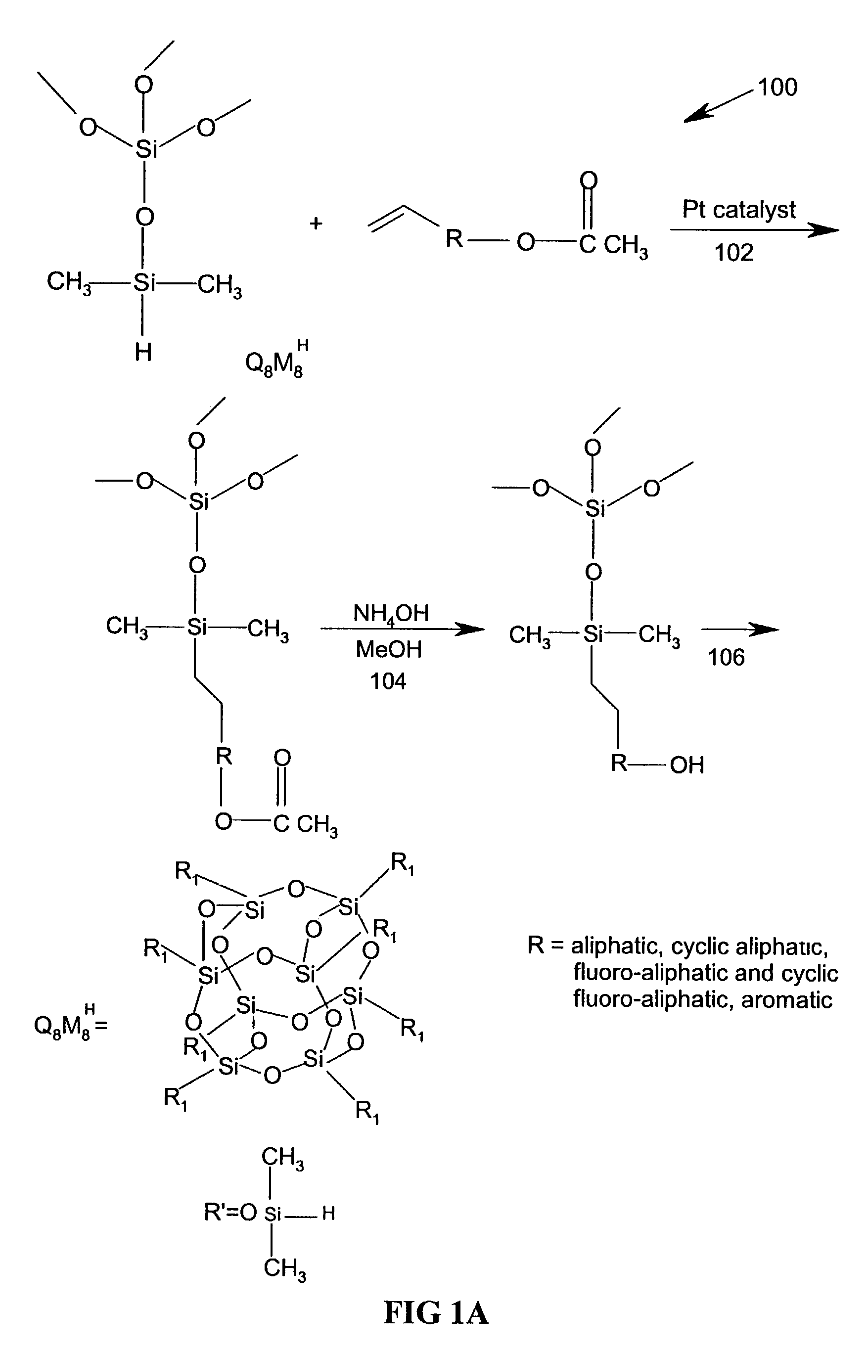
Synthesis of Octakis[(4-hydroxyphenethyl)dimethylsilyloxy]silsesquioxane (CSSQ HPE)

[0105]

Structure 1

[0106]I. Octakis(dimethylsilyloxy)silsesquioxane(Q8M8H) (10.16 grams, 0.01 mole), 4-acetoxystyrene(16.22 g, 0.1 mole) and hexane (100 ml) were placed in a round bottom flask equipped with magnetic stirrer, nitrogen inlet, and a water condensor. Platinum(0)-1,2-divinyl-1,1,3,3-tetramethyldisiloxane complex in xylene (1 ml) was added to this mixture and stirred at room temperature. The reaction became mildly exothermic. After half an hour at room temperature, the solution was heated to reflux for 2 hours. On cooling to room temperature, material separated and settled in the bottom as a waxy solid. This material was rinsed twice with hexane (30 ml) and dried under vacuum.

[0107]II. The above material was heated to reflux with methanol (100 ml) and ammonium hydroxide (14.8 molar) (12 ml, 0.18 mole) for two hours. The progress of the reaction was monitored by IR spectroscopy. The s...

Example

EXAMPLE 2

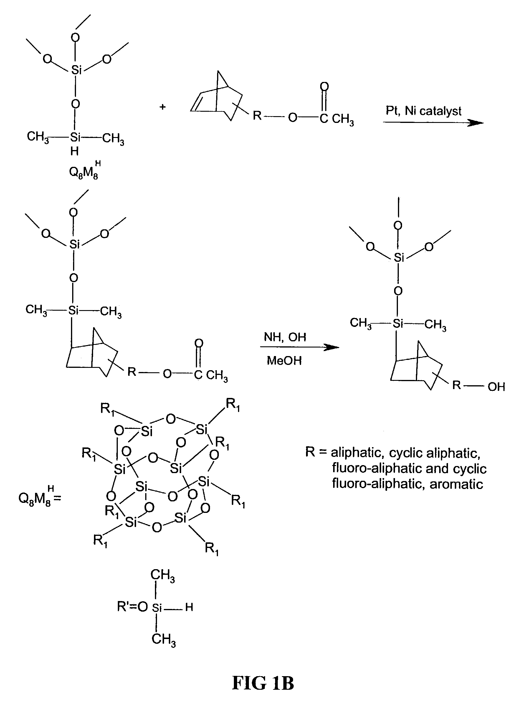
Synthesis of Octakis[{2-(1′,1′-bis(trifluoromethyl)-1′-hydroxyethyl)norbornyl}dimethylsilyloxy]silsesquioxane (Structure 2) (CSSQ NBHFA)

[0110]

Structure 2

[0111]Using a similar procedure as in Example 1, 10.1 grams of Octakis[{2-(1′,1′-bis(trifluoromethyl)-1′-hyroxyethyl)norbornyl}dimethylsilyloxy]silsesquioxane (structure 2) was prepared from Octakis(dimethylsilyloxy)silsesquioxane (Q8M8 11) (5.08 g, 0.005 mole) and 2-(1′,1′-bis(trifluoromethyl)-1′-acetoxyethyl)norbornene (14.2 g, 0.045 mole).

[0112]Notes: 2-(1′,1′-bis(trifluoromethyl)-1′-acetoxyethyl)norbornene was prepared from 2-(1′,1′-bis(trifluoromethyl)-1′-hydroxyethyl)norbornene (Central Glass, Japan), using a standard procedure (acetylchloride and triethyl amine).

Example

EXAMPLE 3

Poly(4-hydroxy-α-methylbenzylsilsesquioxane) (PHMBS)

[0113]A patternable low-k composition was formulated with 1.0 g PHMBS, 0.33 g methylphenyltetramethoxymethyl glycoluril (methylphenyl POWDERLINK), 0.0925 g di(t-butylphenyl)iodonium triflate, 0.14 g of 1 wt. % coumarin-1 in propylene-glycolmonomethylether acetate (PGMEA), 0.067 g of 10% by weight surfactant (FLUORAD FC-430) in PGMEA, and 11.32 g propylene-glycolmonomethylether acetate (PGMEA) solvent. The resulting low-k formulation was filtered wafer and cured at 425° C. for 2 hours under N2 atmosphere. The resultant film had a dielectric constant as measured by MIS structure of 2.99 at 23° C. The dielectric constant, electrical breakdown field of the same film cured at 400° C. had a dielectric constant of 3.4, 5 MV / cm, respectively.


PUM

PropertyMeasurementUnit
Compositionaaaaaaaaaa
Sensitivityaaaaaaaaaa

Abstract

The present invention relates to ultra-large scale integrated (ULSI) interconnect structures, and more particularly to patternable low dielectric constant (low-k) materials suitable for use in ULSI interconnect structures. The patternable low-k dielectrics disclosed herein are functionalized polymers that having one or more acid-sensitive imageable functional groups.

Description

FIELD OF THE INVENTION[0001]The present invention relates to ultra-large scale integrated (ULSI) interconnect structures, and more particularly to patternable low dielectric constant (low-k) materials suitable for use in ULSI interconnect structures. The patternable low-k dielectrics disclosed herein comprise a functionalized polymer having one or more acid-sensitive imageable functional groups. More specifically, the patternable low-k dielectrics of the present invention are based on acid-catalyzed photochemical transformation of silsesquioxane (SSQ)-type polymers under irradiation to achieve patterning capability which are then converted into a low-k material after curing. The present invention also provides a method of integrating the patternable low-k materials of the present invention in semiconductor back-end-of-the-line (BEOL) structures.BACKGROUND OF THE INVENTION[0002]Generally, semiconductor devices include a plurality of integrated circuits (ICs). ICs can be useful for ma...

Claims


Application Information

Patent Timeline
IPC IPC(8): C08L83/04G03F7/075C08G77/04C08G77/14C08G77/24C08K5/00C08L83/06C09D183/08G03F7/004H01L21/312H01L21/316H01L21/3205H01L21/768H01L23/522H01L23/532
CPCC08G77/04C09D183/08G03F7/0046G03F7/0757H01L21/02118H01L21/02126H01L21/02203H01L21/02216H01L21/02282H01L21/02348H01L21/31H01L21/3122H01L21/3124H01L21/31695H01L21/76814H01L21/7682H01L23/5329C08G77/24H01L2924/0002H01L2924/00H01L2221/1047Y10T428/31663G03F7/075
Inventor LIN, QINGHUANGSOORIYAKUMARAN, RATNAM
Owner AURIGA INNOVATIONS INC
Why Eureka
Try Eureka