Printed circuit board and method for manufacturing the same

Active Publication Date: 2014-03-13
LG INNOTEK CO LTD
View PDF18 Cites 4 Cited by
  • Summary
  • Abstract
  • Description
  • Claims
  • Application Information

AI Technical Summary

Benefits of technology

[0012]According to the embodiment, the inner circuit layer and the vias are simultaneously formed, so that the process steps can be reduced. In addition, since the printed circuit board includes odd circuit layers, the printed circuit board may have the light and slim structure.
[0013]In addition, the vias are buried in the insulating layer of the multi-layer printed circ

Problems solved by technology

However, since the number of the circuit pattern layers is limited to the even number, a thickness of the substrate may be increased, so that the multi-la

Method used


Image

  • Printed circuit board and method for manufacturing the same
  • Printed circuit board and method for manufacturing the same
  • Printed circuit board and method for manufacturing the same

Examples


first embodiment

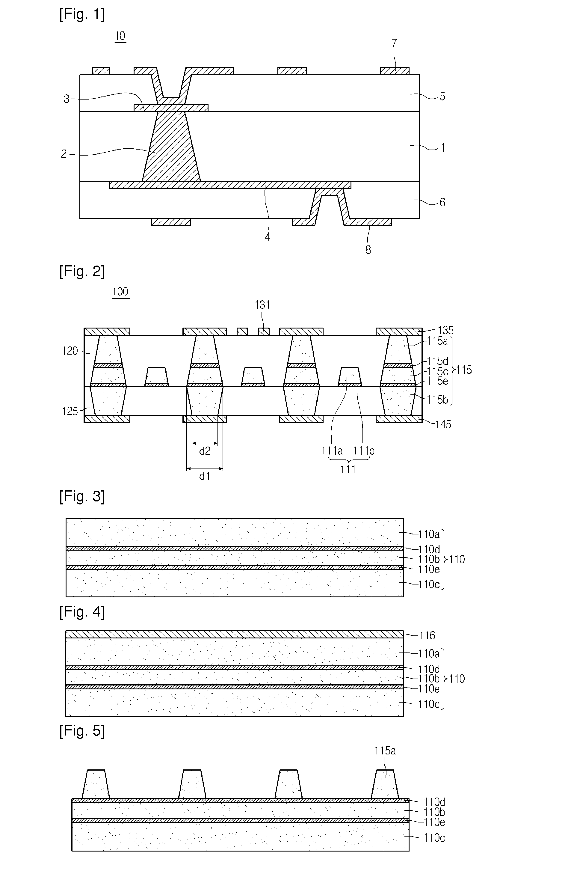
[0029]FIG. 2 is a sectional view showing the PCB according to the

[0030]Referring to FIG. 2, the PCB 100 according to the embodiment includes a core insulating layer forming a first insulating layer 120 and a second insulating layer 125, vias 115 formed in the core insulating layer, an inner circuit layer 111 formed in the core insulating layer, and first and second outer circuit layers 131, 135 and 145 formed on the first and second insulating layers 120 and 125, respectively.

[0031]The first insulating layer 120 is formed on the second insulating layer 125 and an additional insulating layer (not shown) may be present between the first and second insulating layers 120 and 125.

[0032]The first and second insulating layers 120 and 125 may include a thermosetting polymer substrate, a thermoplastic polymer substrate, a ceramic substrate or an organic / inorganic composite substrate. The first and second insulating layers 120 and 125 may include polymer resin, such as epoxy insulating resin,...

second embodiment

[0092]Hereinafter, a PCB will be described with reference to FIG. 18.

[0093]Referring to FIG. 18, the PCB 200 according to the second embodiment includes a core insulating layer forming a first insulating layer 120 and a second insulating layer 125, vias 115 formed in the core insulating layer, an inner circuit layer 112 formed in the core insulating layer, and first and second outer circuit layers 131, 135 and 145 formed on the first and second insulating layers 120 and 125, respectively.

[0094]The first insulating layer 120 is formed on the second insulating layer 125 and an additional insulating layer may be present between the first and second insulating layers 120 and 125.

[0095]The first and second insulating layers 120 and 125 can be formed by using resin including solid components, such as glass fiber. The first and second insulating layers 120 and 125 can be formed by using the same material.

[0096]The first and second insulating layers 120 and 125 have a stack structure to fo...

third embodiment

[0118]Hereinafter, the PCB will be described with reference to FIGS. 19 to 36.

[0119]FIG. 19 is a sectional view showing the PCB according to the third embodiment.

[0120]Referring to FIG. 19, the PCB 300 according to the embodiment includes a core insulating layer forming a first insulating layer 320 and a second insulating layer 325, vias 315 formed in the core insulating layer, an inner circuit layer 311 formed in the core insulating layer, and first and second outer circuit layers 331, 335 and 345 formed on the first and second insulating layers 320 and 325, respectively.

[0121]The first insulating layer 320 is formed on the second insulating layer 325 and an additional insulating layer (not shown) may be present between the first and second insulating layers 320 and 325.

[0122]The first and second insulating layers 320 and 325 may include a thermosetting polymer substrate, a thermoplastic polymer substrate, a ceramic substrate or an organic / inorganic composite substrate. The first ...


PUM


Abstract

Disclosed are a printed circuit board and a method for manufacturing the same. The printed circuit board includes a core insulating layer, at least one via formed through the core insulating layer, an inner circuit layer buried in the core insulating layer, and an outer circuit layer on a top surface or a bottom surface of the core insulating layer, wherein the via includes a first part, a second part below the first part, a third part between the first and second parts, and at least one barrier layer including a metal different from a metal of the first to third parts. The inner circuit layer and the via are simultaneously formed so that the process steps are reduced. Since odd circuit layers are provided, the printed circuit board has a light and slim structure.

Description

TECHNICAL FIELD[0001]A printed circuit board is formed by printing circuit line patterns on an insulating substrate using a conductive material such as copper. The printed circuit board refers to a board before electronic parts have been mounted thereon. That is, the printed circuit board refers to a circuit board, in which mounting positions are defined on a flat plate to mount various types of electronic devices and circuit patterns are fixedly printed on the flat plate to connect the electronic devices with each other.BACKGROUND ART[0002]Such a printed circuit board (PCB) may be classified into a single-layer PCB and a multi-layer PCB, such as a build-up board.[0003]The build-up board, that is, the multi-layer PCB is manufactured one-layer by one-layer and the quality of the multi-layer PCB is evaluated to improve the product yield of the multi-layer PCB. In addition, interconnection lines are precisely connected to manufacture a high-density and small-size PCB. According to the ...

Claims


Application Information

Patent Timeline
IPC IPC(8): H05K1/02H05K3/38H05K3/42H05K3/06
CPCH05K1/0298H05K3/428H05K3/388H05K3/064H05K3/4647H05K3/4652H05K3/4682H05K2201/0341H05K2203/0376H05K2201/0361H05K2203/0384
Inventor LEE, SANG MYUNGYOON, SUNG WOONLEE, HYUK SOOLEE, SUNG WONCHUN, KI DO
Owner LG INNOTEK CO LTD
Why Eureka
Try Eureka