Protective Cover for an Acoustic Wave Device and Fabrication Method Thereof

Inactive Publication Date: 2017-09-21
WIN SEMICON
View PDF0 Cites 5 Cited by
  • Summary
  • Abstract
  • Description
  • Claims
  • Application Information

AI Technical Summary

Benefits of technology

The present invention provides an acoustic wave device protection structure and a formation method to prevent molding compound from affecting the frequency response characteristic during packaging. The protection structure includes a metal covering layer with a concave surface and bottom rim that creates a cavity over the resonant area. A simple process is used to form the protection structure, which is stable and not easy to collapse. The protection structure can be applied using flip chip bonding or wire bonding technology.

Problems solved by technology

Acoustic wave devices are very sensitive to the mass loading.
Even a very small mass loading may change the frequency response of the device.
This is owing to the mass loading on the surface of the device changes the boundary condition of the acoustic wave resonance, which leads to a change of the frequency response characteristic of the device.
However, it is required to use the high price gold bump in the ultrasonic flip chip bonding technology, and the fabrication rate is low.

Method used


Image

  • Protective Cover for an Acoustic Wave Device and Fabrication Method Thereof
  • Protective Cover for an Acoustic Wave Device and Fabrication Method Thereof
  • Protective Cover for an Acoustic Wave Device and Fabrication Method Thereof

Examples


Embodiment Construction

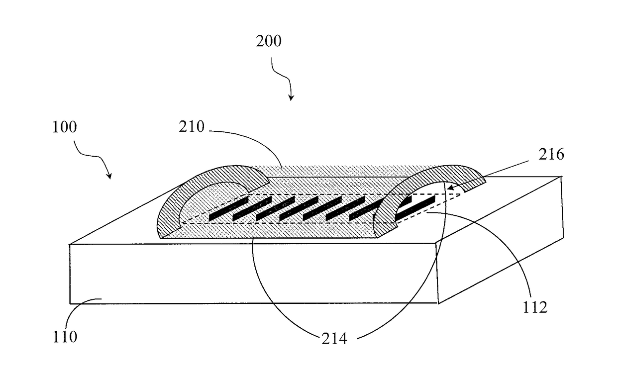
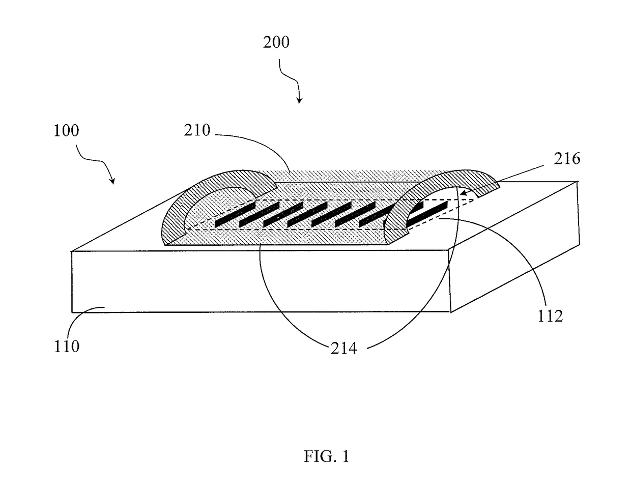
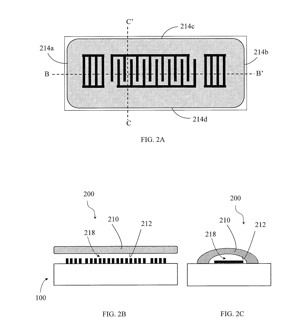
[0034]FIGS. 1A and 2A-2C show an embodiment of an acoustic wave device protection structure provided by the present invention. As shown in the figures, an acoustic wave device 100 comprises a substrate 110 and an interdigital transducer (IDT) on a surface of the substrate 110. The area on the substrate containing the IDT is defined as a resonant area 112. An acoustic wave device protection structure 200 is formed on the acoustic wave device 100 and comprises a metal covering layer 210. The metal covering layer 210 has a concave surface 212 and a bottom rim 214. The bottom rim 214 is connected to the substrate 110 of the acoustic wave device 100 and forms at least one opening 216 between the bottom rim 214 and the acoustic wave device 100. The concave surface 212 covers over the resonant area 112 to form a cavity 218 between the concave surface 212 and the resonant area 112. The formed acoustic wave device protection structure 200 is for protecting the acoustic wave device 100, so as...


PUM


Abstract

A protective cover for an acoustic wave device and a fabrication method thereof, for protecting an acoustic wave device having a resonant area on a surface of a substrate during a packaging operation so as to avoid molding compound flowing onto the resonant area of the acoustic wave device, wherein at least one electrical device is provided on the surface of the substrate and the at least one electrical device includes a temperature sensor. The acoustic wave device protection structure comprising: a metal covering layer, having a concave surface and a bottom rim, the bottom rim connected to the acoustic wave device and forming at least one opening between the bottom rim and the acoustic wave device, and the concave surface covering over the resonant area to form a cavity between the concave surface and the resonant area.

Description

CROSS-REFERENCE TO RELATED DOCUMENTS[0001]This application is a Continuation-in-Part of co-pending application Ser. No. 15 / 070,383, filed on Mar. 15, 2016, for which priority is claimed under 35 U.S.C. §120; and this application claims priority of Application No. 104129984 filed in Taiwan on Sep. 10, 2015 under 35 U.S.C. §119; the entire contents of all of which are hereby incorporated by reference.FIELD OF THE INVENTION[0002]The present invention relates to a protective cover for an acoustic wave device and a fabrication method thereof, and more particular to a method for forming a protective cover for an acoustic wave device used in a communication system and a fabrication method thereof.BACKGROUND OF THE INVENTION[0003]The band pass filter in a communication system is comprised of various acoustic wave devices, including surface acoustic wave filter and bulk acoustic wave filter. Acoustic wave devices are very sensitive to the mass loading. Even a very small mass loading may chan...

Claims


Application Information

Patent Timeline
IPC IPC(8): H03H9/10G01K7/16G01K7/34G01K13/00
CPCH03H9/1071H03H9/1014G01K7/34G01K7/16G01K13/00
Inventor LIN, CHENG-KUOTSAI, SHU-HSIAOSYU, RONG-HAOLIU, YI-LINGLIN, RE-CHINGLIAO, PEI-CHUNCHIANG, CHIH-FENG
Owner WIN SEMICON
Why Eureka
Try Eureka