Through-silicon via interconnection formed with a cap layer

Inactive Publication Date: 2008-12-11
TAIWAN SEMICON MFG CO LTD
View PDF4 Cites 22 Cited by
  • Summary
  • Abstract
  • Description
  • Claims
  • Application Information

AI Technical Summary

Benefits of technology

[0013]The advantageous features of the present invention includes reduced process steps, and he

Problems solved by technology

Although dramatic improvements in lithography have resulted in considerable improvements in 2D integrated circuit formation, there are physical limitations to the density that can be achieved in two dimensions.
One of these limitations is the minimum size needed to make these components.
Also, when more devices are put into one chip, more complex designs

Method used


Image

  • Through-silicon via interconnection formed with a cap layer
  • Through-silicon via interconnection formed with a cap layer
  • Through-silicon via interconnection formed with a cap layer

Examples


Example

[0017]The making and using of the presently preferred embodiments are discussed in detail below. It should be appreciated, however, that the present invention provides many applicable inventive concepts that can be embodied in a wide variety of specific contexts. The specific embodiments discussed are merely illustrative of specific ways to make and use the invention, and do not limit the scope of the invention.

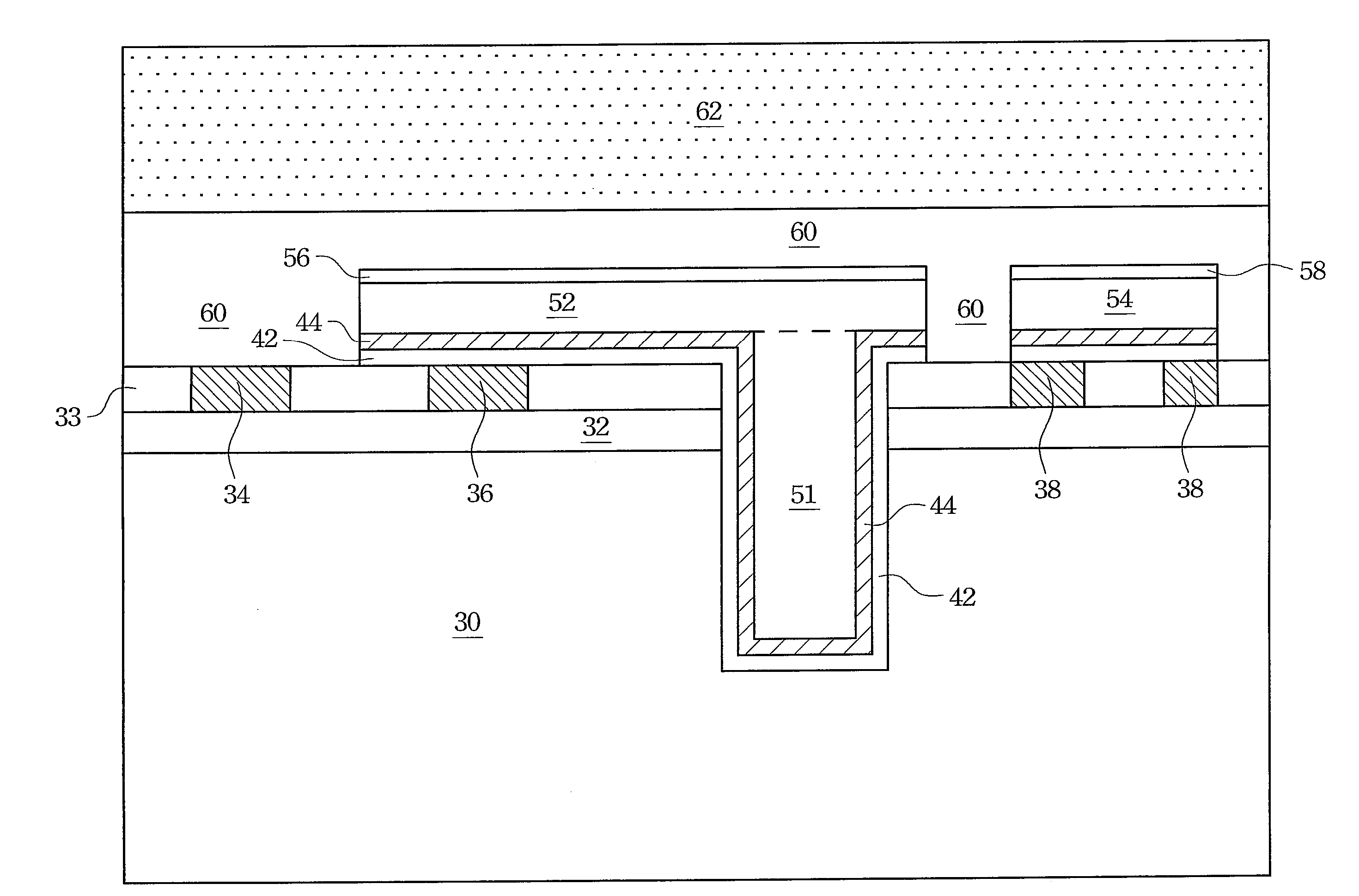
[0018]A novel method for forming through-silicon vias is provided. The intermediate stages of manufacturing a preferred embodiment of the present invention are illustrated. Throughout the various views and illustrative embodiments of the present invention, like reference numbers are used to designate like elements.

[0019]Referring to FIG. 4, a wafer including base material 30 is provided. Base material 30 preferably includes a semiconductor substrate, such as bulk silicon substrate. Other semiconductor materials including group III, group IV and group V elements may also be us...


PUM


Abstract

An integrated circuit structure and methods for forming the same are provided. The method includes providing a substrate; forming a through-silicon via (TSV) opening extending into the substrate; forming an under-bump metallurgy (UBM) in the TSV opening, wherein the UBM extends out of the TSV opening; filling the TSV opening with a metallic material; forming a patterned cap layer on the metallic material; and etching a portion of the UBM outside the TSV opening, wherein the patterned cap layer is used as a mask.

Description

TECHNICAL FIELD[0001]This invention relates generally to integrated circuits, and more particularly to structures and manufacturing methods of through-silicon vias.BACKGROUND[0002]Since the invention of integrated circuits, the semiconductor industry has experienced continuous rapid growth due to constant improvements in the integration density of various electronic components (i.e., transistors, diodes, resistors, capacitors, etc.). For the most part, this improvement in integration density has come from repeated reductions in minimum feature size, allowing more components to be integrated into a given chip area.[0003]These integration improvements are essentially two-dimensional (2D) in nature, in that the volume occupied by the integrated components is essentially on the surface of the semiconductor wafer. Although dramatic improvements in lithography have resulted in considerable improvements in 2D integrated circuit formation, there are physical limitations to the density that ...

Claims


Application Information

Patent Timeline
IPC IPC(8): H01L23/528H01L21/4763
CPCH01L21/6836H01L21/76898H01L23/53238H01L24/05H01L2221/6834H01L2924/01078H01L2924/01079H01L2924/01322H01L2924/04941H01L2924/14H01L2924/19041H01L2924/19043
Inventor HUANG, HON-LINSU, BOETSENG, LI-HSINCHENG, CHIA-JENYU, HSIU-MEI
Owner TAIWAN SEMICON MFG CO LTD
Why Eureka
Try Eureka