
Display panel

A technology for display panels and substrates, which is used in static indicators, instruments, identification devices, etc., can solve the problem of difficulty in improving the resolution of display panels, and achieve the effect of increasing circuit layout space, increasing resolution or space utilization.

Active Publication Date: 2021-02-23
AU OPTRONICS CORP
View PDF8 Cites 0 Cited by
  • Summary
  • Abstract
  • Description
  • Claims
  • Application Information

AI Technical Summary

Problems solved by technology

However, limited by the number of transistors in the pixel circuit, it is increasingly difficult to improve the resolution of the display panel, so a new display panel structure is required

Method used


Image

  • Display panel
  • Display panel
  • Display panel

Examples


Embodiment Construction

[0056] Unless otherwise defined, all terms (including technical and scientific terms) used herein have the same meaning as commonly understood by one of ordinary skill in the art to which this invention belongs. It will be further understood that terms such as those defined in commonly used dictionaries should be interpreted to have meanings consistent with their meanings in the context of the relevant art and the present invention, and will not be interpreted as idealized or excessive formal meaning, unless expressly so defined herein.

[0057] It should be understood that although the terms "first", "second", "third" etc. may be used herein to describe various elements, components, regions, layers and / or sections, these elements, components, regions, and and / or parts should not be limited by these terms. These terms are only used to distinguish one element, component, region, layer or section from another element, component, region, layer or section. Thus, "a first element...


PUM


Abstract

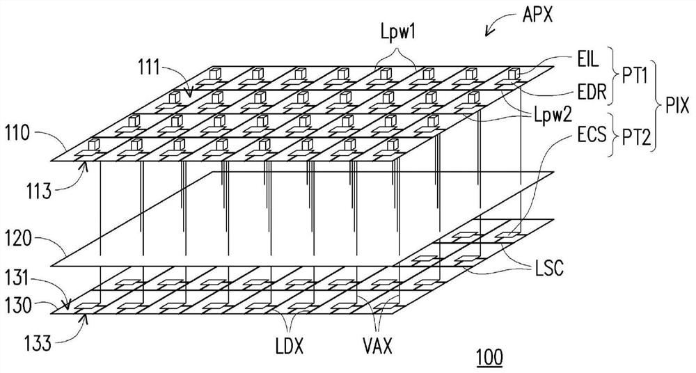
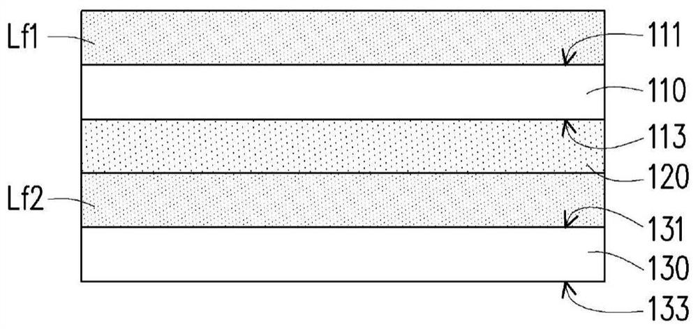
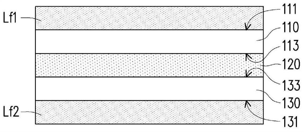
A display panel comprises a first substrate, a second substrate, a plurality of pixel circuits and a plurality of through holes. The first substrate has a first surface and a second surface opposite to the first surface. The second substrate has a third surface and a fourth surface opposite to the third surface. The pixel circuits are respectively provided with a first part and a second part, thefirst parts of the pixel circuits are arranged on the first surface in an array mode, and the second parts of the pixel circuits are arranged on the third surface in an array mode. The through holes are formed in the first substrate and the second substrate so as to be electrically connected with the first part and the second part of each pixel circuit.

Description

technical field [0001] The present invention relates to a display panel, and in particular to a display panel with high pixel density. Background technique [0002] With the gradual popularity of mobile phone color screens, the material of mobile phone screens is becoming more and more important. The color screens of mobile phones vary due to different screen materials and development technologies. The types generally include thin film transistor liquid crystal display (TFT), thin film diode semitransparent (Thin Film Diode, TFD), UFB, ultra Twisted nematic (Super Twisted Nematic, STN) and organic light emitting diode (Organic Light Emitting Display, OLED) and so on. Generally speaking, in addition to the color gamut of the display panel, the higher the resolution of the display panel, the more complex images can be displayed, and the layers of the picture can be enriched. However, limited by the number of transistors in the pixel circuit, it is increasingly difficult to i...

Claims


Application Information

Patent Timeline
Patent Type & Authority Applications(China)
IPC IPC(8): G09F9/33G09G3/3208
CPCG09F9/33G09G3/3208
Inventor 黄景亮洪嘉泽郭庭玮郑君丞
Owner AU OPTRONICS CORP
Learn More