Unlock instant, AI-driven research and patent intelligence for your innovation.

Object identifying method, object identifying circuit and sampling circuit

一种辨识方法、物件的技术,应用在光学物件辨识领域,能够解决降低指纹影像精确度、产生漏电流、占据感测结果动态范围等问题,达到提升动态范围的效果

Pending Publication Date: 2021-03-05
NOVATEK MICROELECTRONICS CORP
View PDF0 Cites 0 Cited by
  • Summary
  • Abstract
  • Description
  • Claims
  • Application Information

AI Technical Summary

Problems solved by technology

However, when the photodiode is not illuminated by light, there will still be a slight leakage current, which is called dark current.
No photocurrent will greatly occupy the dynamic range of the sensing result, thus reducing the accuracy of the fingerprint image

Method used


Image

  • Object identifying method, object identifying circuit and sampling circuit
  • Object identifying method, object identifying circuit and sampling circuit
  • Object identifying method, object identifying circuit and sampling circuit

Examples


Embodiment Construction

[0058] Embodiments of the disclosed document will be described below with reference to the accompanying drawings. In the drawings, the same reference numerals represent the same or similar elements or method flows.

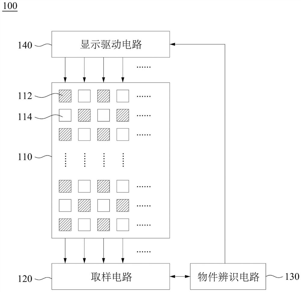
[0059] figure 1It is a simplified functional block diagram of the object recognition system 100 according to an embodiment of the disclosed document. The object recognition system 100 includes a display panel 110 , a sampling circuit 120 , an object recognition circuit 130 and a display driving circuit 140 . In some embodiments, the object recognition circuit 130 is disposed under the display panel 110 . The object recognition system 100 is used for sensing an image of an object under test contacting a surface of the display panel 110 . For example, the object recognition system 100 can be used to implement optical fingerprint sensing. In order to make the drawing concise and easy to explain, other components and connection relationships in the object recognit...


PUM


Abstract

The invention relates to an object identifying method, an object identifying circuit and a sampling circuit. The object identifying method, suitable for an object identifying circuit configured to bedisposed under a display panel, includes the following operations: displaying a black pattern by the display panel; generating a plurality of first sensing signals of a plurality of first sensor pixels of the display panel arranged in the black pattern; generating a plurality of second sensing signals of a plurality of second sensor pixels of the display panel arranged in a contact area with whichthe display panel contacting an object to be identified; adjusting voltage levels of the plurality of second sensing signals according to the plurality of first sensing signals; and generating an image corresponding to the object to be identified from the adjusted plurality of second sensing signals. One of the advantages of the object identifying method is to increase the dynamic range of a light sensing result.

Description

technical field [0001] The disclosed document relates to an object identification method, especially an optical object identification method. Background technique [0002] In order to make the product more beautiful, mobile devices often adopt the design of disposing the optical fingerprint sensing module under the display panel, or integrate the optical fingerprint sensing module into the display panel to realize a full-screen design. The optical fingerprint sensing module senses the leakage current generated by the photodiode exposed to the light reflected by the fingertip to generate a fingerprint image. However, when the photodiode is not illuminated by light, it still generates a slight leakage current, which is called dark current. No photocurrent will greatly occupy the dynamic range of the sensing result, thus reducing the accuracy of the fingerprint image. Contents of the invention [0003] The disclosure document provides an object identification method, which ...

Claims


Application Information

Patent Timeline
Patent Type & Authority Applications(China)
IPC IPC(8): G06K9/00G06F3/041G09G3/36G09G3/3208H01L27/32
CPCG06F3/0412G09G3/36G09G3/3208G06V40/1318H10K59/65G09G2354/00G09G2310/0245G09G2360/144G09G3/20G09G3/3225G09G3/3607
Inventor 陈季廷
Owner NOVATEK MICROELECTRONICS CORP
Features
  • R&D
  • Intellectual Property
  • Life Sciences
  • Materials
  • Tech Scout
  • Unparalleled Data Quality
  • Higher Quality Content
  • 60% Fewer Hallucinations
Learn More