Method for mapping digital-analog pin of analog layout to digital layout

A technology of layout and model introduction, applied in the fields of electrical digital data processing, special data processing applications, instruments, etc., can solve problems such as affecting the chip design cycle, repeated iteration of layout design, and consuming the time and energy of layout designers.

Pending Publication Date: 2021-03-16
AMICRO SEMICON CORP
View PDF1 Cites 5 Cited by
  • Summary
  • Abstract
  • Description
  • Claims
  • Application Information

AI Technical Summary

Problems solved by technology

This traditional method not only requires the analog layout designer to accurately count the digital and analog pin information, but also requires the digital layout designer to accurately transfer the pin information contained in the text information to the digita

Method used


Image

  • Method for mapping digital-analog pin of analog layout to digital layout
  • Method for mapping digital-analog pin of analog layout to digital layout
  • Method for mapping digital-analog pin of analog layout to digital layout

Examples


Embodiment Construction

[0017] The technical solutions in the embodiments of the present invention will be described in detail below with reference to the drawings in the embodiments of the present invention. It should be understood that the specific embodiments described below are only used to explain the present invention, not to limit the present invention.

[0018] Those skilled in the art can understand that, unless otherwise defined, all terms (including technical terms and scientific terms) used in the specification have the same meanings as commonly understood by those of ordinary skill in the art to which this invention belongs. It should also be understood that terms such as those defined in commonly used dictionaries should be understood to have meanings consistent with the meanings in the context of the prior art, and will not be used in idealized or overly formal meanings unless specifically defined. Explanation.

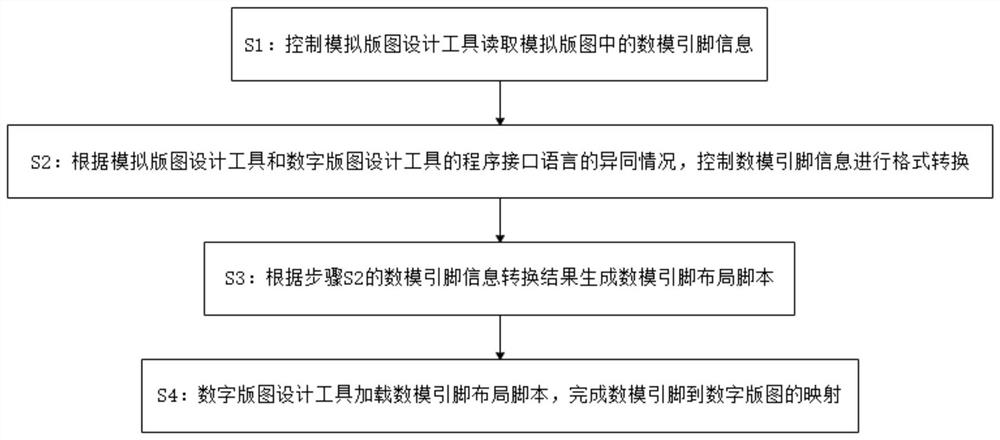
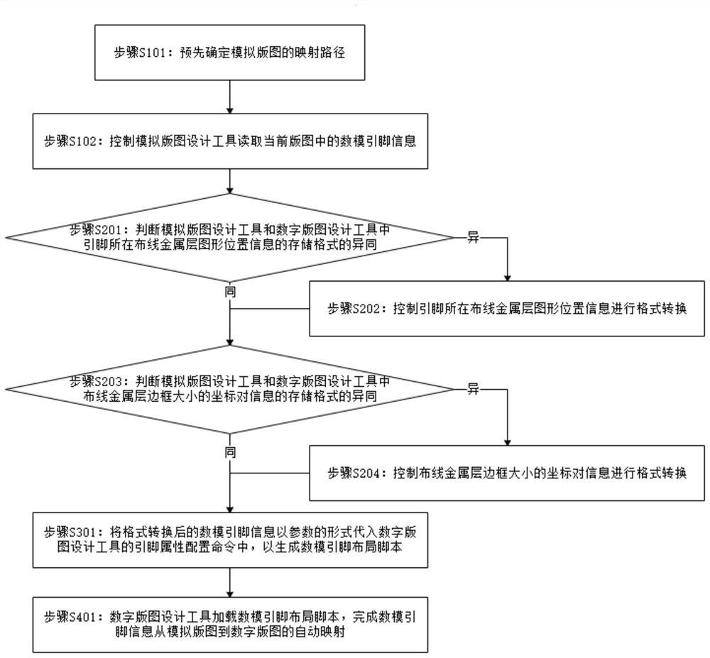
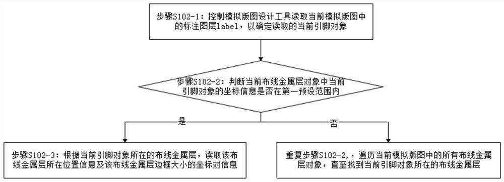
[0019]An embodiment of the present invention provides a method for mappi...


PUM


Abstract

The invention discloses a method for mapping a digital-analog pin of an analog layout to a digital layout. The method comprises the following steps of: 1, controlling an analog layout design tool to read digital-analog pin information of the analog layout; 2, controlling the digital-analog pin information read in the step 1 to perform format conversion according to program interface language similarities and differences corresponding to the analog layout design tool and the digital layout design tool; 3, controlling the digital-analog pin information to generate a digital-analog pin layout script according to the format conversion result in the step 2; and step 4, controlling a digital layout design tool to load the digital-analog pin layout script according to the digital-analog pin layout script generated in the step 3, and completing mapping of the digital-analog pin to the digital layout. According to the method, automatic mapping of the digital-analog pin information in the designof the analog layout package digital layout is realized, so that the time and energy consumed by a layout designer in the layout stage are reduced, and the processing period of information interaction of the digital template graph is greatly shortened.

Description

technical field [0001] The invention relates to the field of layout information interaction, in particular to a method for mapping digital and analog pins of an analog layout to a digital layout. Background technique [0002] Integrated circuits, also known as IC (Intergrated Circuit), can be divided into three categories: analog integrated circuits, digital integrated circuits, and digital-analog hybrid integrated circuits according to their functions and structures. Among them, the design of digital-analog hybrid integrated circuits can be divided into two methods: digital package analog design and analog package digital design. Chip-level layout design method. In the layout design of digital-analog hybrid integrated circuits, due to the different design tools used in digital layout and analog layout, when completing digital-analog mixing, it is necessary to provide information interaction between digital layout and analog layout to complete both digital and analog. inte...

Claims


Application Information

Patent Timeline
IPC IPC(8): G06F30/392
CPCG06F30/392
Inventor 蔡晓銮黄明强
Owner AMICRO SEMICON CORP
Why Eureka
Try Eureka