
JTAG data capture and analysis system

An analysis system and data capture technology, applied in the direction of electrical digital data processing, instruments, and faulty computer hardware detection, can solve problems such as logic design errors, affecting the efficiency of software and hardware debugging, and JTAG unable to communicate normally.

Pending Publication Date: 2021-03-19
XIAN UNIV OF POSTS & TELECOMM
View PDF0 Cites 0 Cited by
  • Summary
  • Abstract
  • Description
  • Claims
  • Application Information

AI Technical Summary

Problems solved by technology

[0003] Computer processor JTAG circuit logic design errors, emulator signal distortion, JTAG clock frequency is too high, and target processor board-level circuit design errors will cause JTAG to fail to communicate normally. Software and hardware engineers often need to spend a lot of time analyzing and finding that JTAG cannot communicate normally. The reasons affect the debugging efficiency of software and hardware

Method used


Image

  • JTAG data capture and analysis system
  • JTAG data capture and analysis system
  • JTAG data capture and analysis system

Examples


Embodiment Construction

[0024] In order to make the purpose, technical solutions and advantages of the embodiments of the present invention more clear, the implementation manners of the present invention will be described in detail below in conjunction with the drawings and embodiments.

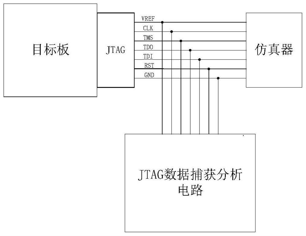
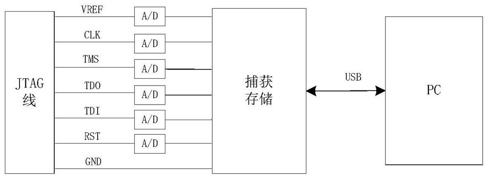
[0025] The invention is a JTAG data capturing and analyzing system, which is mainly used for diagnosing the communication failure of the JTAG debugging interface. refer to figure 2 , during the debugging process for the target processor, it is installed between the target processor and the emulator, connected to each communication signal line of the JTAG debugging interface, independent of the target processor and the emulator, and connected externally between the two Collect the JTAG communication signals, and analyze and detect communication faults based on the collected signals.

[0026] Specifically, the system of the present invention includes three main modules, as follows:

[0027] The JTAG communication s...


PUM


Abstract

A JTAG data capture and analysis system comprises a JTAG communication signal acquisition sub-module, a communication signal analysis and communication protocol analysis sub-module and a user interaction sub-module. The JTAG communication signal acquisition sub-module acquires a JTAG communication signal between a target processor and a simulator through an ADC. The communication signal analysis and communication protocol analysis sub-module diagnoses a communication fault existing between the target processor and the simulator by analyzing the waveform of each signal in a JTAG debugging interface and communication data of a higher layer, and determines a fault source between two communication parties. The user interaction sub-module displays the wrong communication signal and the failed communication protocol and gives a fault diagnosis result. The fault source in JTAG communication is diagnosed by analyzing the communication protocol of the JTAG debugging interface, so that the debugging efficiency of the processor is improved.

Description

technical field [0001] The invention belongs to the technical field of computer system debugging, in particular to a JTAG data capture and analysis system. Background technique [0002] Computer processors typically debug / emulate and download programs via JTAG. In the FPGA verification stage, sample test stage and user board-level design stage, the processor needs to establish normal communication between the emulator and the target processor through JTAG, and then the subsequent hardware debugging simulation and program download can be performed, such as figure 1 shown. The normal operation of the JTAG communication circuit is the basis for the subsequent debugging of the processor chip. However, traditional debugging methods such as oscilloscopes have problems such as slow debugging efficiency and high reliance on hardware engineer debugging experience. [0003] Computer processor JTAG circuit logic design errors, emulator signal distortion, JTAG clock frequency is too h...

Claims


Application Information

Patent Timeline
IPC IPC(8): G06F13/38G06F13/42G06F11/22
CPCG06F13/385G06F13/4282G06F11/221Y02P90/02
Inventor 张琼
Owner XIAN UNIV OF POSTS & TELECOMM
Learn More