Check patentability & draft patents in minutes with Patsnap Eureka AI!

MRAM-NAND controller and data writing method thereof

A MRAM-NAND, controller technology, applied in the field of memory, can solve the problems of long writing time, limited applicability, incompatibility of host chips, etc. Effect

Active Publication Date: 2021-04-13
SHANGHAI CIYU INFORMATION TECH
View PDF3 Cites 0 Cited by
  • Summary
  • Abstract
  • Description
  • Claims
  • Application Information

AI Technical Summary

Problems solved by technology

[0005]However, the existing MRAM reads very fast, no less than DRAM, but the writing time is relatively long, more than ten times that of DRAM
As a result, when the host performs MRAM read / write operations, the timing design cannot achieve the same or similar design to DRAM, that is, it is different from the current working timing of DRAM-related function chips, which is different from the host chips on the market. Compatibility issues not only limit the applicability, but also affect the promotion of products

Method used


Image

  • MRAM-NAND controller and data writing method thereof
  • MRAM-NAND controller and data writing method thereof
  • MRAM-NAND controller and data writing method thereof

Examples


Embodiment Construction

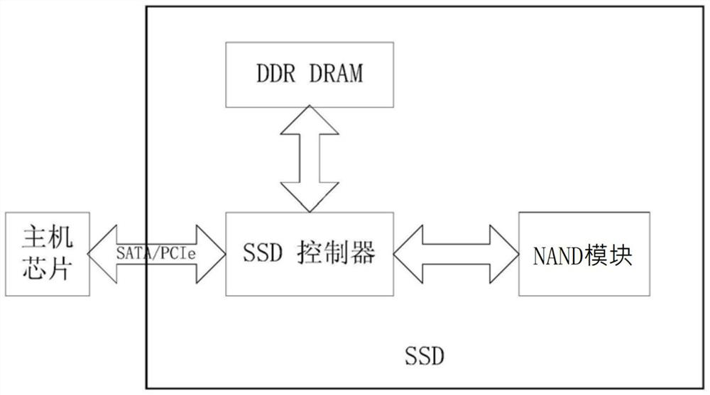
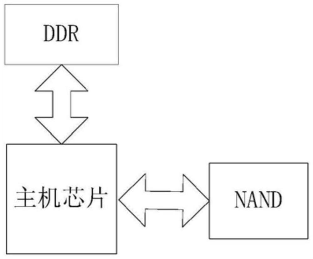
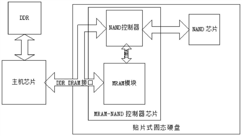
[0029] Please refer to the drawings in the accompanying drawings, wherein like reference numerals refer to like components. The following description is based on illustrated specific embodiments of the present application, which should not be construed as limiting other specific embodiments of the present application that are not described in detail here.

[0030] The following descriptions of the various embodiments refer to the attached drawings to illustrate specific embodiments that the present application can be implemented in. The directional terms mentioned in this application, such as "up", "down", "front", "rear", "left", "right", "inside", "outside", "side", etc., are for reference only The orientation of the attached schema. Therefore, the directional terms used are used to illustrate and understand the application, but not to limit the application.

[0031] The terms "first", "second", "third", etc. (if any) in the description and claims of this application and t...


PUM


Abstract

The invention provides an MRAM-NAND controller and a data writing method thereof. The controller comprises an embedded MRAM, a host interface adopting a DDRD-RAM interface standard, an NAND controller, a microcontroller, a buffer and a state register. Due to the fact that the DDR-DRAM interface is adopted as the host interface of the MRAM-NAND controller, the read-write speed of the controller and the read-write speed of a memory bank applied to the controller can be increased. Through caching, the read / write operation efficiency of the controller chip can be effectively improved and stabilized, meanwhile, the working time sequence is adjusted to cope with the compatibility problem of an existing host chip, and the applicability of related products can be improved.

Description

technical field [0001] This application relates to the field of memory technology, in particular to an MRAM-NAND controller and a data writing method thereof. Background technique [0002] Solid State Drives (SSD), referred to as solid disks, are hard disks made of solid-state electronic storage chip arrays, consisting of a control unit and a storage unit (FLASH chip, DRAM chip). The specifications and definitions of interfaces, functions and usage methods of solid-state hard disks are exactly the same as those of ordinary hard disks, and the shape and size of the products are also completely consistent with ordinary hard disks. It is widely used in military, vehicle, industrial control, video surveillance, network monitoring, network terminals, electric power, medical, aviation, navigation equipment and other fields. [0003] Although the development of NAND flash memory technology has promoted the SSD industry, due to the strict requirements on size, it is difficult for e...

Claims


Application Information

Patent Timeline
IPC IPC(8): G06F3/06
CPCG06F3/061G06F3/0656G06F3/0658G06F3/0688Y02D10/00
Inventor 戴瑾
Owner SHANGHAI CIYU INFORMATION TECH
Features
  • R&D
  • Intellectual Property
  • Life Sciences
  • Materials
  • Tech Scout
  • Unparalleled Data Quality
  • Higher Quality Content
  • 60% Fewer Hallucinations
Learn More