Method for increasing reading and writing speeds of NAND flash controller

A technology of read and write speed and controller, applied in instruments, memory systems, memory address/allocation/relocation, etc., can solve the problems of underutilization of chip cache resources, reduce read and write speed, increase cost, etc., and achieve flexible cache Operation mode, the effect of improving the reading and writing speed

Active Publication Date: 2014-02-05
SHANDONG UNIV
View PDF7 Cites 20 Cited by
  • Summary
  • Abstract
  • Description
  • Claims
  • Application Information

AI Technical Summary

Problems solved by technology

[0003] At present, the commonly used method to improve the read and write speed of the NAND flash controller is to set up a cache inside the controller, and increase the speed of random read and write by setting a large number of caches, but this method will bring about a problem: while increasing the speed, it will reduce the cost. Greatly improve
[0004] Patent No.: 200710164187.9, Inventor: Que Jinzhen, Patent Name: "NAND FLASH Controller and Its Data Interaction Method with NAND FLASH Chip" discloses a data interaction method between a NAND FLASH controller and a NAND FLASH chip. The structure of the controller It is a more commonly used control structure at present, and its data buffer only plays the role of "receiving the information data transmitted by the system bus through the bus timing interface", while NAND flash must be read in units of pages when performing read and write operations. Writing, if you do not use a large amount of cache when reading and writing NAND flash, the reading and writing speed will be greatly reduced; if you can use these data buffer resources when reading and writing operations, the reading and writing speed will be improved to a certain extent
The cache resources in the chip are not fully utilized, which is a defect in the existing technology

Method used


Image

  • Method for increasing reading and writing speeds of NAND flash controller

Examples


Embodiment

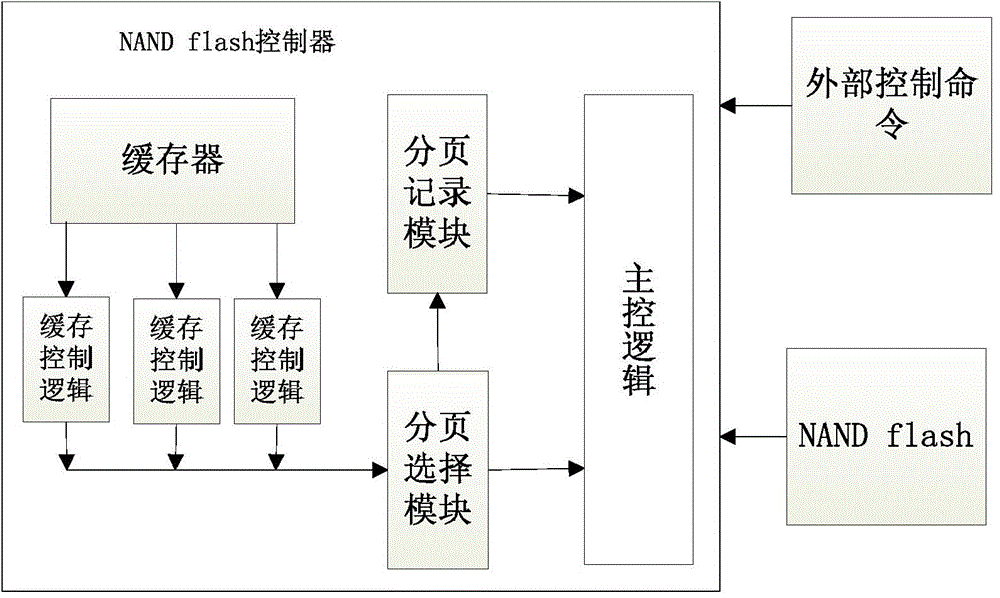
[0026] Such as figure 1 As shown, a method for improving the read and write speed of the NAND flash controller is realized by the following system, the system includes the NAND flash controller, NAND flash and external control commands, one end of the NAND flash controller is connected to the system bus, and the other end It is directly connected with NAND flash, and external control commands can directly operate the NAND flash controller; the NAND flash controller includes main control logic, a buffer, multiple sets of cache control logic, a paging selection module and a paging recording module, the main control logic With ECC verification module; the cache is used to cache the read and write data, and the cache control logic is connected with the cache for dynamic allocation of the cache; the paging selection module is connected with the cache control logic and the main control logic for Select the currently used cache page in the cache page, which can be set by an external ...


PUM


Abstract

The invention discloses a method for increasing the reading and writing speeds of an NAND flash controller, and belongs to the technical field of integrated circuit design. One end of the NAND flash controller is connected to a system bus, and the other end of the NAND flash controller is directly connected with a NAND flash. The method comprises the following steps: reading the parameter of a page size from the NAND flash; dynamically allocating cache inside the NAND flash controller to generate a plurality of cache sub-pages adapting to the page size of the NAND flash; selecting a current cache sub-page via an external control command; selecting a current cache page to allow the external control command to directly operate the current cache page. The method has the advantages that the controller can well adapt to different models of NAND flash, the own limited cache resources are utilized to the maximum extent, a more flexible cache operating way is provided for the external control command, and the reading and writing speeds of the NAND flash are increased.

Description

technical field [0001] The invention relates to a method for improving the reading and writing speed of the controller to the NAND flash device by dynamically configuring the paging size of the internal cache of the NAND flash controller, belonging to the technical field of digital integrated circuit design. Background technique [0002] With the integration of chips getting higher and higher, today's mobile phones, tablet computers, etc. are integrated with commonly used digital functions such as Internet access, games, music playback, video playback, and photography. higher requirement. Flash is currently the most commonly used non-volatile memory. In terms of the use of Flash, NAND Flash has a lower unit bit cost than NOR Flash, greater storage density, faster writing and erasing speed, and more The advantages of more erasable times. However, due to the complex interface timing of NAND flash, and the operation can only be performed in units of pages when reading and wri...

Claims


Application Information

Patent Timeline
Patent Type & Authority Applications(China)
IPC IPC(8): G06F12/08G06F13/14G06F12/0871
Inventor 周莉孙皓孙涛陈鹏董启凡马召宾汪洋
Owner SHANDONG UNIV
Why Eureka
Try Eureka