Optical splicing imaging device

An imaging device and optical splicing technology, which is applied in optics, optical components, instruments, etc., can solve the problems of limited caliber and energy loss of the optical system, and achieve the effects of increasing the field of view, compressing the volume, and ensuring machinability

Inactive Publication Date: 2021-04-27
CHANGCHUN INST OF OPTICS FINE MECHANICS & PHYSICS CHINESE ACAD OF SCI
View PDF6 Cites 0 Cited by
  • Summary
  • Abstract
  • Description
  • Claims
  • Application Information

AI Technical Summary

Problems solved by technology

[0004] In view of the above problems, the purpose of the present invention is to provide an optical splicing imaging device to solve the problem of the traditional mechanical splicing method having a blind area of ​​the field of view and the traditional optical splicing method having energy loss, which leads to the limitation of the aperture of the optical system.

Method used


Image

  • Optical splicing imaging device
  • Optical splicing imaging device
  • Optical splicing imaging device

Examples


Embodiment Construction

[0029] In order to make the object, technical solution and advantages of the present invention clearer, the present invention will be further described in detail below in conjunction with the accompanying drawings and specific embodiments. It should be understood that the specific embodiments described here are only used to explain the present invention, but not to limit the present invention.

[0030] The structure of the optical splicing imaging device provided by the present invention will be described in detail below with specific embodiments.

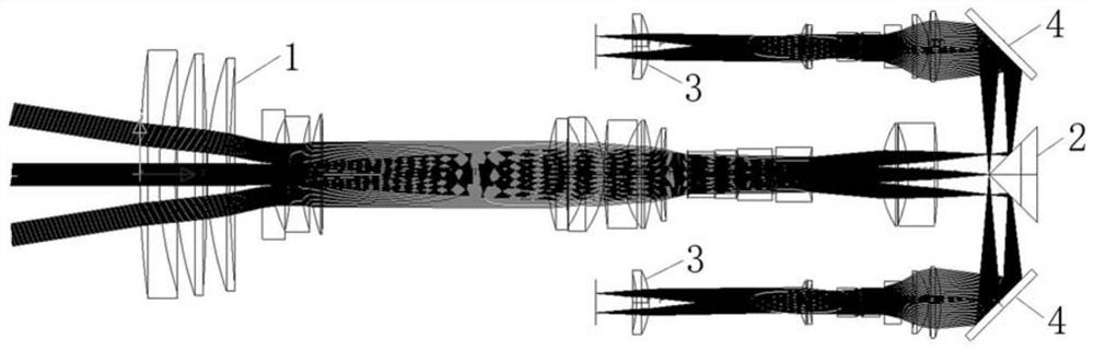
[0031] image 3 Shown is the overall structure of an optical splicing imaging device according to an embodiment of the present invention.

[0032] Such as image 3 As shown, the optical splicing imaging device provided by the embodiment of the present invention includes: a primary imaging optical system 1, a spectroscopic element 2 and two secondary imaging optical systems 3, the primary imaging optical system 1 is used for prima...


PUM


Abstract

The invention provides an optical splicing imaging device which comprises a primary imaging optical system and two secondary imaging optical systems; wherein a light splitting element is arranged on a primary image surface of the primary imaging optical system; an image formed by the primary imaging optical system on the primary image surface is divided into two parts after being reflected by the light splitting element and respectively enters two secondary imaging optical systems to carry out secondary imaging; wherein the light splitting element is provided with two reflecting surfaces which are perpendicular to each other, an included angle of 45 degrees is formed between each of the two reflecting surfaces and an incident light beam, and the intersection of the two reflecting surfaces is located on a primary image surface. According to the invention, seamless splicing of the field of view is achieved in an optical splicing mode without field-of-view blind area; so that the energy loss can be reduced to the minimum through arrangement of the light splitting element, and therefore the requirement for the relative aperture of an optical system is lowered, and the machinability of the lens is guaranteed.

Description

technical field [0001] The invention relates to the technical field of micro-nano preparation, in particular to an optical splicing imaging device. Background technique [0002] With the development of optical systems and imaging detection devices, users expect optical detection equipment to have both high resolution and large field of view capabilities. Under the premise that the target surface size of the imaging detector is fixed, increasing the focal length of the optical system can improve the detail resolution of the image, but the field of view observed by the system will be proportionally reduced, so a larger-sized image sensor is required to improve the optical system. Field of view, however, it is difficult to process and manufacture large-size and high-resolution image sensors, so a multi-sensor splicing process is often used to improve the field of view. [0003] The multi-sensor splicing process includes mechanical splicing and optical splicing. Such as figur...

Claims


Application Information

Patent Timeline
IPC IPC(8): G02B13/00G02B27/14G02B15/14G02B15/15G02B13/22G02B13/06
CPCG02B13/00G02B13/06G02B13/22G02B15/15G02B27/143G02B15/144
Inventor 刘韬徐首龙
Owner CHANGCHUN INST OF OPTICS FINE MECHANICS & PHYSICS CHINESE ACAD OF SCI
Why Eureka
Try Eureka