
Pixel driving circuit and display panel

A technology of pixel driving circuit and display panel, which is applied in the field of display device manufacturing, pixel driving circuit and display panel, can solve the problems of MicroLED with large minimum value, multiple gray levels, and unrealizable pixels.

Inactive Publication Date: 2021-06-04
SHENZHEN CHINA STAR OPTOELECTRONICS SEMICON DISPLAY TECH CO LTD
View PDF8 Cites 2 Cited by
  • Summary
  • Abstract
  • Description
  • Claims
  • Application Information

AI Technical Summary

Problems solved by technology

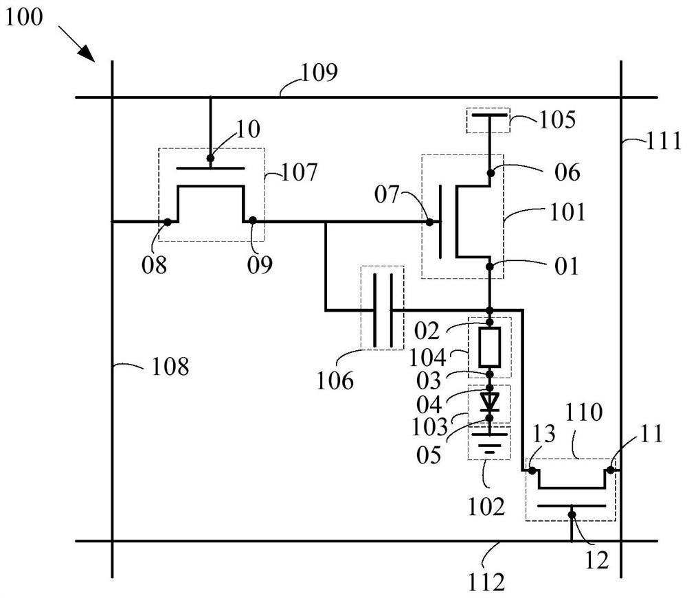
[0004] The embodiment of the present application provides a pixel drive circuit and a display panel. By connecting the adjustment module in series on the branch of the light-emitting module, the minimum value of the voltage change of the Micro LED caused by the large change value of the voltage output of the existing drive module is large. , resulting in the problem that the corresponding pixels cannot achieve a large number of gray levels

Method used


Image

  • Pixel driving circuit and display panel
  • Pixel driving circuit and display panel
  • Pixel driving circuit and display panel

Examples


Embodiment Construction

[0029] The technical solutions in the embodiments of the present application will be clearly and completely described below in conjunction with the drawings in the embodiments of the present application. Apparently, the described embodiments are only some of the embodiments of this application, not all of them. Based on the embodiments in this application, all other embodiments obtained by those skilled in the art without making creative efforts belong to the scope of protection of this application.

[0030] In the description of the present invention, it should be understood that the orientation or positional relationship indicated by the terms "upper", "lower", etc. is based on the orientation or positional relationship shown in the drawings, for example, "upper" means that the surface is above the object, Specifically, it can refer to directly above, obliquely above, or the upper surface, as long as it is above the level of the object; "both sides" or "both ends" refer to t...


PUM

PropertyMeasurementUnit
electrical resistivityaaaaaaaaaa
thicknessaaaaaaaaaa
thicknessaaaaaaaaaa

Abstract

The invention provides a pixel driving circuit and a display panel, the pixel driving circuit comprises a driving module, a first voltage module, a light-emitting module and an adjusting module, the two ends of the light-emitting module are electrically connected with the driving module and the first voltage module respectively, the light-emitting module comprises a micro light-emitting diode, and the adjusting module and the light-emitting module are connected in series; and according to the scheme, the adjusting module is connected to the branch of the light emitting module in series, the minimum value of voltage changes at the two ends of the micro light emitting diode can be reduced in an auxiliary mode, the pixel corresponding to the micro light emitting diode can achieve more gray scale levels, the color expressive force of a picture is enriched, and the color level of the picture is increased.

Description

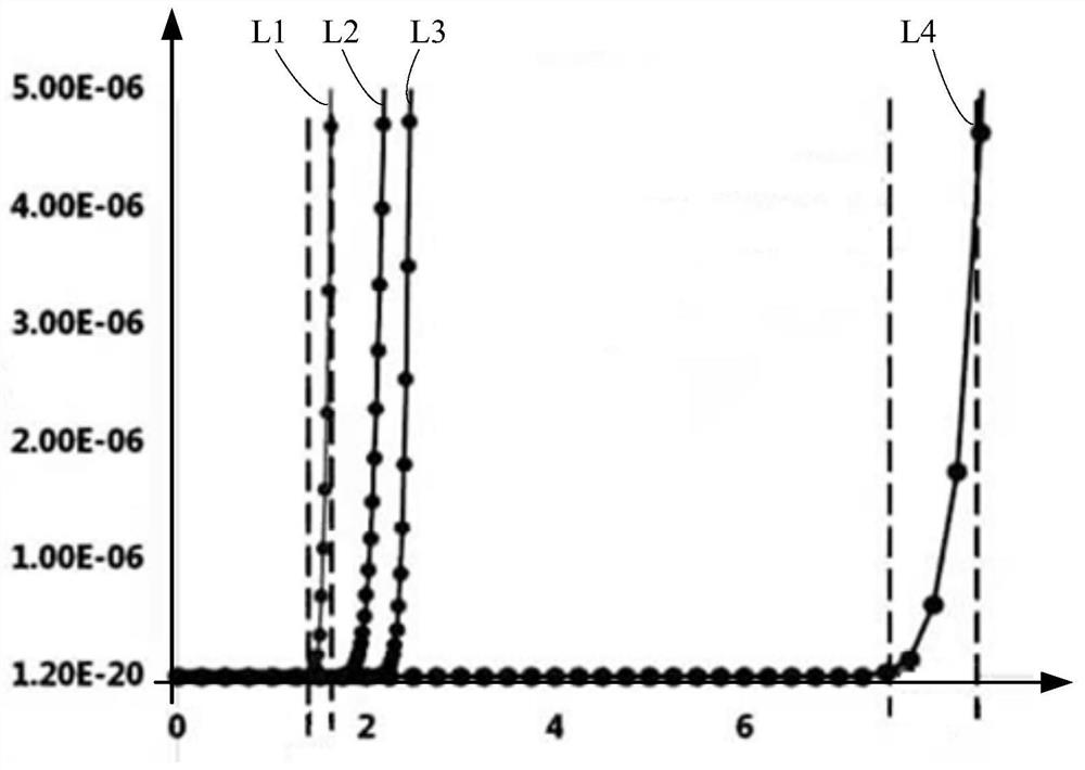
technical field [0001] The present application relates to the field of display technology, in particular to the manufacture of display devices, in particular to pixel drive circuits and display panels. Background technique [0002] Micro LED (Micro Light Emitting Diode, Micro Light Emitting Diode Display), as a new generation display device, has higher brightness, better luminous efficiency and lower power consumption than the existing OLED (Organic Light Emitting Diode, Organic Light Emitting Diode Display). [0003] Such as figure 1 As shown, L1, L2, and L3 are the current-voltage curves of red Micro LED, green Micro LED, and blue Micro LED, respectively, and L4 is the current-voltage curve of OLED. Specifically, the abscissa indicates the corresponding Micro LED or OLED The voltage at both ends, the vertical axis represents the current flowing through the corresponding Micro LED or OLED. Depend on figure 1 It can be seen that the current-voltage curve of Micro LED is s...

Claims


Application Information

Patent Timeline
Patent Type & Authority Applications(China)
IPC IPC(8): G09G3/32
CPCG09G3/32
Inventor 樊勇
Owner SHENZHEN CHINA STAR OPTOELECTRONICS SEMICON DISPLAY TECH CO LTD
Learn More