Check patentability & draft patents in minutes with Patsnap Eureka AI!

Semiconductor processing apparatus having linear conveyor system

A technology of conveying system and processing device, applied in conveyor control device, semiconductor/solid-state device manufacturing, storage device, etc., can solve problems such as semiconductor device defect, failure, uneven copper layer, etc.

Inactive Publication Date: 2003-11-26
APPLIED MATERIALS INC
View PDF0 Cites 0 Cited by
  • Summary
  • Abstract
  • Description
  • Claims
  • Application Information

AI Technical Summary

Problems solved by technology

This in turn may make the copper layer subsequently electroplated on the seed layer non-uniform
This non-uniformity can cause chipping or failure of the formed semiconductor device

Method used


Image

  • Semiconductor processing apparatus having linear conveyor system
  • Semiconductor processing apparatus having linear conveyor system
  • Semiconductor processing apparatus having linear conveyor system

Examples


Embodiment Construction

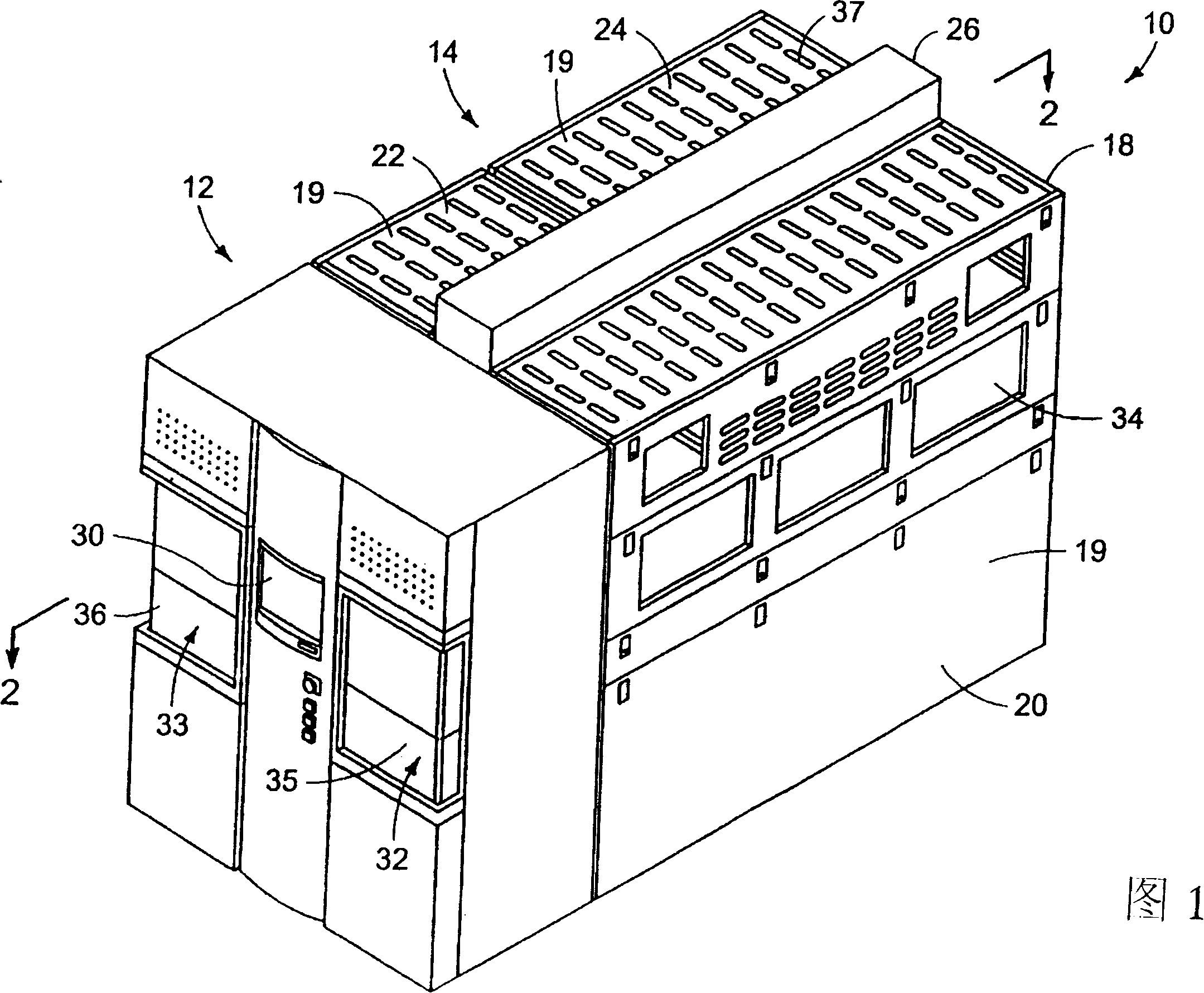
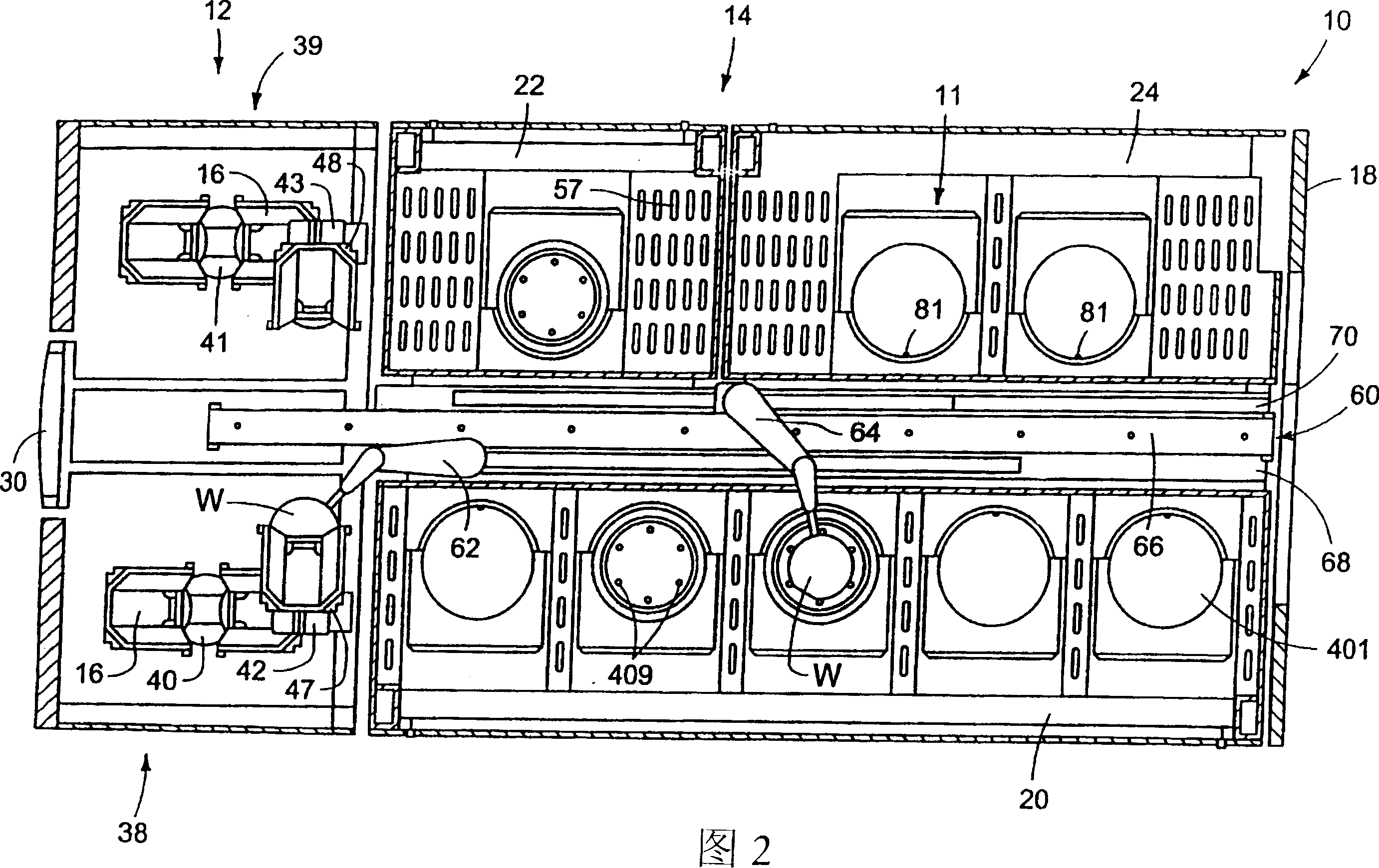
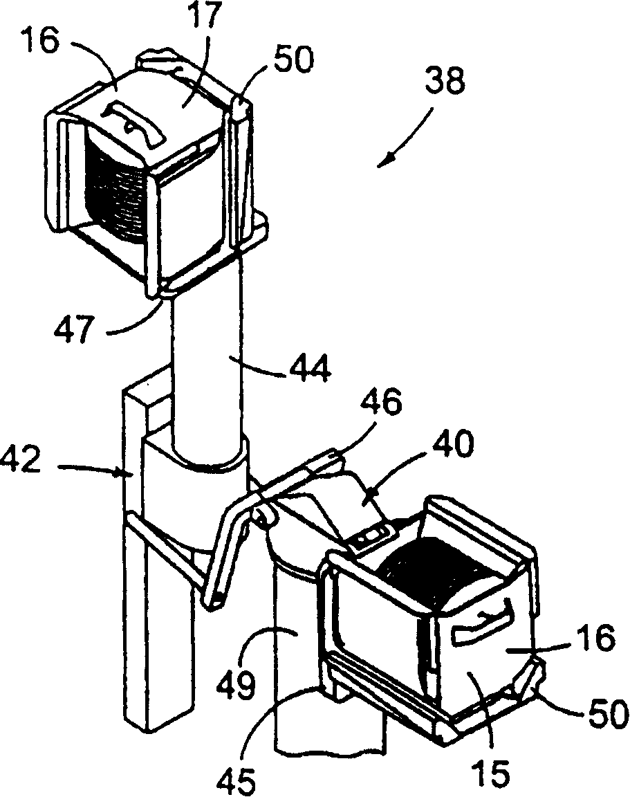
[0024] Referring to FIG. 1, a presently preferred embodiment of a semiconductor wafer processing tool 10 is shown. The processing tool 10 may include an interface portion 12 and a processing portion 14 . A semiconductor wafer cassette 16 containing a plurality of semiconductor wafers, generally designated W, may be loaded into or unloaded from the processing tool 10 through the interface portion 12 . In particular, loading or unloading of wafer cassette 16 is preferably done through at least one port, such as first port 32, in the front exterior surface of the wall facing process tool 10. An additional second port 33 may be provided in the interface portion 12 of the processing tool 10 to improve access, port 32 may be used as an input port and port 33 may be used as an output port.

[0025] The access ports 32, 33 may be covered with respective powered doors 35, 36, thereby isolating the interior of the process tool 10 from the clean room. Each door 35, 36 may comprise two ...


PUM


Abstract

Processing tools, components of tools, and methods of making and using such devices for electrochemical processing of microelectronic workpieces. One aspect of the invention is directed toward reaction vessels for electrochemical processing of microelectronic workpieces, processing stations including such reaction vessels, and methods for using these devices. For example, one embodiment of a reaction vessel includes an outer container having an outer wall, a first outlet configured to introduce a primary fluid flow into the outer container, and at least one second outlet configured to introduce a secondary fluid flow into the outer container separate from the primary fluid flow. The reaction vessel can also include at least one electrode, and it can also have a field shaping unit. The field shaping unit, for example, can be a dielectric assembly coupled to the second outlet to receive the secondary flow and configured to contain the secondary flow separate from the primary flow through at least a portion of the outer container. The field shaping unit can also have at least one electrode compartment through which the secondary flow can pass separately from the primary flow. The electrode is positioned in the electrode compartment.

Description

technical field [0001] This application relates to semiconductor processing devices. Background technique [0002] In the manufacture of semiconductor integrated circuits and other semiconductor products from semiconductor wafers, it is often necessary to provide multiple metal layers on the wafer for use as interconnect metallization to electrically interconnect the various devices on the integrated circuit. Aluminum is commonly used for this interconnection, however, copper metallization has been found to be preferable. [0003] In particular, the application of copper on semiconductor wafers has proven to be a major technical challenge. At the same time, copper metallization has not been commercialized due to practical problems in reliably and cost-effectively forming copper layers on semiconductor devices. This is partly because reactive ion etching or other selective removal of copper is more difficult to implement at reasonable production temperatures. It is desirab...

Claims


Application Information

Patent Timeline
IPC IPC(8): B65G1/00B65G37/00B65G49/07H01L21/00H01L21/677
CPCH01L21/67742H01L21/67259H01L21/67781H01L21/67769
Inventor 凯尔·汉森马克·迪克斯丹尼尔·J·伍德拉夫韦恩·J·施密特凯文·W·科伊尔
Owner APPLIED MATERIALS INC
Features
  • R&D
  • Intellectual Property
  • Life Sciences
  • Materials
  • Tech Scout
  • Unparalleled Data Quality
  • Higher Quality Content
  • 60% Fewer Hallucinations
Learn More