Method and device for growing silicon carbide crystal by pvt method

A technology of silicon carbide and crystal growth, which is applied in the field of growing silicon carbide crystals by PVT method, which can solve the influence of the uniform stability of the temperature field at the seed crystal, increase the probability of polytype and inclusion generation, disrupt the orderly transmission of silicon carbide atmosphere, etc. problem, to achieve the effect of improving effective utilization, reducing thickness difference, and improving thickness uniformity

Active Publication Date: 2022-07-12
SICC CO LTD
View PDF7 Cites 0 Cited by
  • Summary
  • Abstract
  • Description
  • Claims
  • Application Information

AI Technical Summary

Problems solved by technology

[0005] In the existing method of raising and lowering the crucible during the crystal growth process, the temperature field at the seed crystal can be adjusted and controlled by adjusting the position of the crucible, but the lifting and lowering of the crucible will also seriously affect the uniformity and stability of the temperature field at the seed crystal. Disrupt the orderly transmission of silicon carbide atmosphere, and cause the silicon carbide powder in the crucible to vibrate and shift, significantly increase the probability of defects such as polymorphism and inclusions, and reduce the crystallization quality of silicon carbide, etc.

Method used


Image

  • Method and device for growing silicon carbide crystal by pvt method
  • Method and device for growing silicon carbide crystal by pvt method
  • Method and device for growing silicon carbide crystal by pvt method

Examples


Embodiment 1

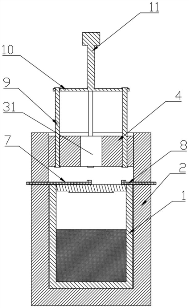
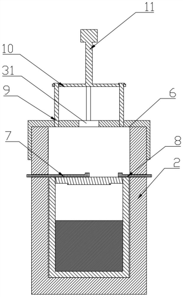
[0064] refer to Figure 1-4 , this embodiment provides a crystal growth device, the device includes a crucible 1, a holding cylinder 2 and a furnace body, the bottom of the crucible 1 is used for placing silicon carbide raw materials, and the top of the crucible 1 is used for setting seed crystals; the holding cylinder 2 has A hollow cavity with one end open and the other closed; the crucible 1 is placed in the hollow cavity; the top of the heat preservation cover 3 is provided with a heat dissipation hole 31, the heat preservation cover 3 is arranged at the opening of the heat preservation cylinder 2, and the side wall of the heat preservation cover 3 is connected to the heat preservation cylinder. The top side wall of 2 abuts, and the heat preservation cover 3 can move along the top side wall of the heat preservation cylinder 2. The heat preservation cover 3 is provided with a heat dissipation hole 31; the furnace body is used for placing the crucible 1 and the heat preservat...

Embodiment 2

[0080] A method for growing silicon carbide crystals using the device described in Embodiment 1, the method comprising the steps of:

[0081](1) Assembly stage: the seed crystal is placed on the top of the crucible, and the silicon carbide raw material is filled at the bottom of the crucible; the crucible and the heat preservation cylinder are assembled, the assembled crucible is placed in the furnace body of the crystal growth furnace and sealed, and the bottom of the heat preservation cover is sealed. The distance from the top cover of the crucible is L, and L is 10-300mm;

[0082] (2) Impurity removal stage: vacuum the furnace body to 10 -6 Below mbar, then pass high-purity inert gas to 300~500mbar, repeat this process 2~3 times, and finally vacuum the furnace body to 10 -6 Below mbar;

[0083] (3) Heating stage: control the temperature of the first temperature measuring device at the top center of the crucible to rise to T1 and synchronously increase the pressure to P1, ...


PUM


Abstract

The invention provides a method and device for growing silicon carbide crystal by PVT method. The method includes: (1) an assembly stage; (2) a heating stage: the assembled crucible is placed in a furnace body, and the crucible is heated, The temperature difference between the temperature at the center of the top of the crucible and the edge of the top of the crucible is controlled to be ΔT1; (3) Crystal growth stage: keep the temperature at the center of the top of the crucible unchanged, control the heat preservation cover to move up along the side wall of the heat preservation cylinder, and control the center of the top of the crucible at the same time. The temperature difference between the temperature of the crucible and the top edge of the crucible is reduced to ΔT2, so that the silicon carbide raw material gas phase is transferred to the seed crystal for crystal growth. By controlling the upward movement of the heat preservation cover, the annular temperature field is more uniform and stable, and the radial temperature gradient gradually decreases to ΔT2, realizing the directional quantitative adjustment of the radial temperature gradient, gradually reducing the radial temperature gradient at the seed crystal, and reducing the size of the silicon carbide. The difference between the minimum thickness of the center and the edge of the crystal increases the effective utilization of the same weight of silicon carbide crystal.

Description

technical field [0001] The invention relates to a method and a device for growing silicon carbide crystals by PVT method, and belongs to the technical field of semiconductor material preparation. Background technique [0002] Silicon carbide crystal is a typical wide-bandgap semiconductor material, and it is one of the representatives of the third-generation semiconductor materials after silicon and gallium arsenide. Silicon carbide crystal has excellent properties such as high thermal conductivity, high breakdown field strength, and high saturation electron mobility, and has become one of the popular materials for preparing high-temperature, high-frequency, high-power and radiation-resistant devices. [0003] At present, the methods of silicon carbide growth mainly include physical vapor transport (PVT), liquid phase epitaxy (LPE), chemical vapor deposition (CVD), etc. Among them, PVT method is the most mature method. The growth furnace for the growth of silicon carbide cr...

Claims


Application Information

Patent Timeline
Patent Type & Authority Patents(China)
IPC IPC(8): C30B29/36C30B23/00
CPCC30B29/36C30B23/00
Inventor 李加林刘星李斌孙元行刘鹏飞李博侯建国刘家朋
Owner SICC CO LTD
Why Eureka
Try Eureka