

Solid-state imaging device and electronic apparatus
A solid-state imaging device and electrode technology, which is applied in the direction of electric solid-state devices, radiation control devices, televisions, etc., can solve the problems of saturation signal volume and reduction, and achieve the effect of improving saturation characteristics
- Summary
- Abstract
- Description
- Claims
- Application Information
AI Technical Summary
Problems solved by technology
Method used
Image

Examples
Deformed example 1
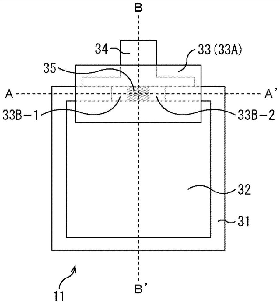
[0077] Figure 10 with Figure 11 Another configuration example of the pixel 11 is illustrated. Figure 10 is a plan view illustrating this configuration example of the pixel 11 . Figure 11 yes Figure 10 shown in Pixel 11 with image 3 The sectional view corresponding to the sectional view.
[0078] At the same time, in Figure 10 with Figure 11 , are designated with the same reference numerals as the image 3 with Figure 4 constructions similar to those in , and descriptions of these constructions are omitted.
[0079] The transfer gate electrode 51 is obtained by integrally forming the planar gate electrode 51A and the vertical gate electrodes 51B- 1 , 51B- 2 , and 51B- 3 . The planar gate electrode 51A is formed across the PD 32 and the FD 34 on the semiconductor substrate 31 . The vertical gate electrodes 51B- 1 , 51B- 2 , and 51B- 3 are formed to have a columnar shape in the depth direction from the surface of the semiconductor substrate 31 in a region betwe...
Deformed example 2
[0083] Figure 12 with Figure 13 Still another configuration example of the pixel 11 is illustrated. Figure 12 is a plan view illustrating this configuration example of the pixel 11 . Figure 13 yes Figure 12 shown in Pixel 11 with image 3 The sectional view corresponding to the sectional view.
[0084] At the same time, in Figure 12 with Figure 13 , are designated with the same reference numerals as the image 3 with Figure 4 constructions similar to those in , and descriptions of these constructions are omitted.
[0085] The transfer gate electrode 61 is obtained by integrally forming the planar gate electrode 61A and the vertical gate electrodes 61B- 1 , 61B- 2 , and 61B- 3 . The planar gate electrode 61A is formed across the PD 32 and the FD 34 on the semiconductor substrate 31 . The vertical gate electrodes 61B- 1 , 61B- 2 , and 61B- 3 are formed to have a columnar shape in the depth direction from the surface of the semiconductor substrate 31 below the p...
Deformed example 3
[0089] Figure 14 with Figure 15 Still another configuration example of the pixel 11 is illustrated. Figure 14 is a plan view illustrating this configuration example of the pixel 11 . Figure 15 yes Figure 14 shown in Pixel 11 with image 3 The sectional view corresponding to the sectional view.
[0090] At the same time, in Figure 14 with Figure 15 , are designated with the same reference numerals as the image 3 with Figure 4 constructions similar to those in , and descriptions of these constructions are omitted.
[0091] The transfer gate electrode 71 is obtained by integrally forming the planar gate electrode 71A and the vertical gate electrodes 71B- 1 , 71B- 2 , and 71B- 3 . The planar gate electrode 71A is formed across the PD 32 and the FD 34 on the semiconductor substrate 31 . The vertical gate electrodes 71B- 1 , 71B- 2 , and 71B- 3 are formed to have a columnar shape in the depth direction from the surface of the semiconductor substrate 31 below the p...
PUM
 Abstract
Description
Claims
Application Information