Display
A display and photosensitive sensor technology, applied in static indicators, instruments, electrical solid devices, etc., can solve problems such as inability to detect and realize functions, and achieve the effects of reducing parasitic capacitance, improving saturation characteristics, and improving detection sensitivity
- Summary
- Abstract
- Description
- Claims
- Application Information
AI Technical Summary
Problems solved by technology
Method used
Image
Examples
no. 1 example
[0079] Now, taking a liquid crystal display as an example and referring to the drawings, a display according to a first embodiment of the present invention will be described below.
[0080] The display of this embodiment is preferably applied to a so-called "transmissive type" liquid crystal display in which light is projected from the backside surface side (the surface side on the opposite side to the frontside surface on which an image is displayed). Therefore, the following description is based on the assumption that the liquid crystal display is a transmissive type.
[0081] (overall structure)
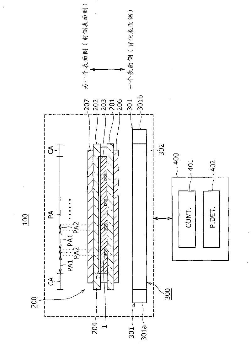
[0082] figure 1 It is a schematic diagram of the overall structure of a transmissive liquid crystal display.
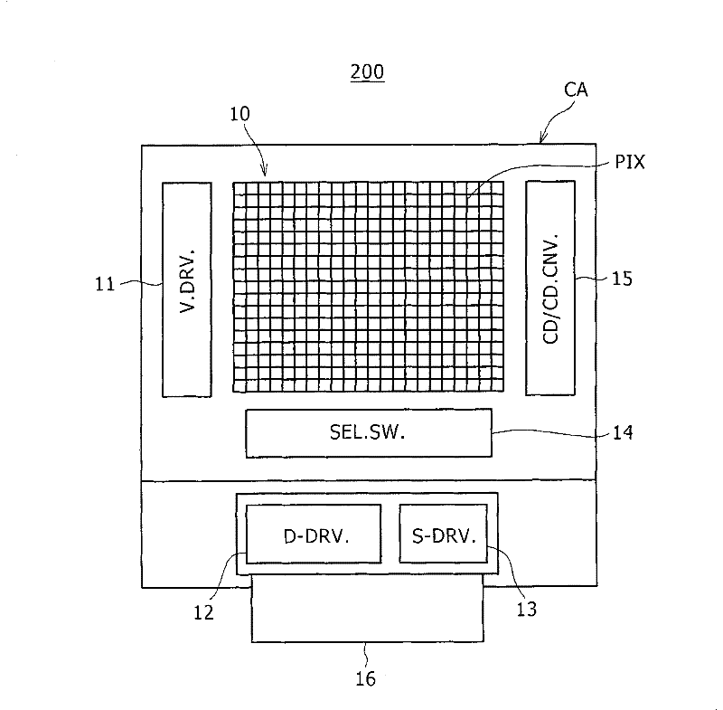
[0083] figure 1 The illustrated liquid crystal display 100 has, for example, a liquid crystal panel 200 as a display section as a "substrate" and a backlight 300 as a "illumination section", and a data processing section 400 .
[0084] For example, if figure 1As show...
example 1
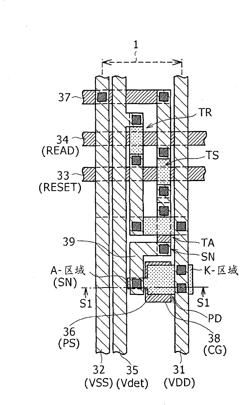
[0262] about Figure 5A and 5B The thin film photodiode shown, manufactured the thin film photodiode according to the existing example, wherein the anode region (P + area) the width Wp of 36A and the cathode area (N + Regions) 36K each have a width Wn equal to 100 μm.
[0263] Here, by shorting the anode region (P + area) 36A and the cathode area (N + region) 36K to test the dependence of the gate capacitance Cg on the voltage Vg applied to the control gate viewed from the gate terminal. Here, set in the anode region (P + area) 36A and the cathode area (N + The widths of the I regions 36I between regions) 36K vary to 4.5 μm (a), 5.5 μm (b), 6.5 μm (c), 7.5 μm (d), 8.5 μm (e) and 9.5 μm (f). In this case, the control gate and cathode region (N + region) 36K and the overlap between the control gate and the anode region (P + The overlap between regions) 36A remains unchanged.
[0264] The results of the above tests are as follows Figure 13 shown.
[0265] When a cert...
example 2
[0271] based on Figure 5A and 5B The structure of the thin film photodiode shown, by setting the cathode region (N + area) 36K has a width Wn of 100 μm, while the variable anode area (P + The width Wp of the area) 36A is used to manufacture a thin film photodiode, and the variation of the parasitic capacitance Cp with the width Wp is measured.
[0272] The result is as Figure 15 , where (a) represents the parasitic capacitance viewed from the control gate 38, and (b) represents the parasitic capacitance viewed from the anode region (P + Area) 36A to see the parasitic capacitance.
[0273] It can be seen from the figure that between the control grid 38 and the cathode region (N + region) 36K connected to each other, the parasitic capacitance component seen from the control gate 38 and the anode region (P + Area) 36A view of the parasitic capacitance components are along with the anode area (P + area) 36A decreases in width. Therefore, it was confirmed that reducing th...
PUM
 Abstract
Description
Claims
Application Information


