A pam4 transmitter driving circuit for high-speed optical interconnection
A driving circuit and optical interconnection technology, which is applied in the direction of electromagnetic transmitters, electrical components, electromagnetic wave transmission systems, etc., can solve the problems of gate circuits limiting high-speed performance, patents that have not been released, and large chip areas, etc., and achieve good application prospects. The effect of saving circuit bandwidth and good signal transmission quality
- Summary
- Abstract
- Description
- Claims
- Application Information
AI Technical Summary
Problems solved by technology
Method used
Image


Examples
Embodiment 1
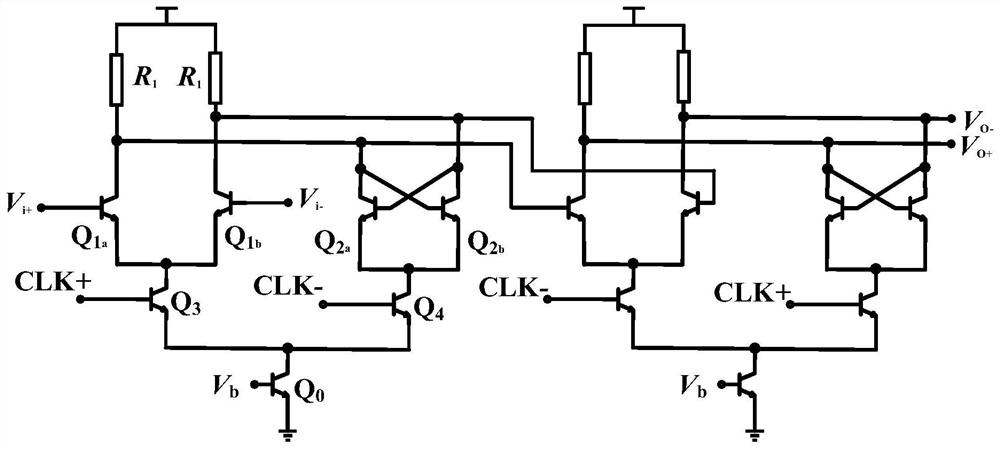
[0041] The embodiment of the present invention proposes a PAM4 transmitter drive circuit for high-speed optical interconnection, see figure 1 , the circuit consists of:
[0042]Four input buffer stages to provide the input impedance matching of the circuit;
[0043] Four D flip-flops, sampling and retiming the input signal to eliminate the possible phase difference;
[0044] Two 2:1 multiplexers to convert four 25Gb / s NRZ signals into two 50Gb / s NRZ signals;
[0045] Two broadband amplifiers to shape the output signal of the multiplexer and increase the bandwidth;
[0046] A CML adder superimposes two NRZ signals into one PAM4 signal, doubling the single-channel data transmission rate.
[0047] A broadband output buffer stage provides circuit output impedance matching and at the same time integrates two bandwidth expansion methods to increase the bandwidth of the entire transmission path.
Embodiment 2
[0049] figure 1 It is the structure diagram of PAM4 transmitter drive circuit. The four 25Gb / s NRZ signals are buffered by the input buffer stage, and the signals are sampled and retimed by the D flip-flop. The retimed signals are respectively multiplexed by two 2:1 multiplexers to obtain two 50Gb / s The NRZ signal, the two signals are amplified and shaped by the broadband amplifier, and then the signals are superimposed by the current mode logic (CML) adder to obtain a PAM4 signal, and the PAM4 signal is buffered by the broadband output buffer stage and output.
[0050] Described in detail below figure 1 The specific realization form of key circuit modules in the structure diagram.
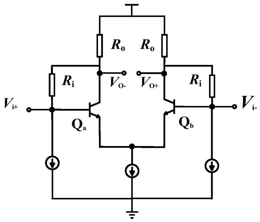
[0051] figure 2 Circuit diagram for the input buffer stage. The overall differential structure is used to suppress the influence of noise on the output; the input signal is connected to the differential pair Q a , Q b The base and collector of the output node V respectively O- , V O+ . A...
PUM
 Abstract
Description
Claims
Application Information
 - R&D
- Intellectual Property
- Life Sciences
- Materials
- Tech Scout
- Unparalleled Data Quality
- Higher Quality Content
- 60% Fewer Hallucinations
Browse by: Latest US Patents, China's latest patents, Technical Efficacy Thesaurus, Application Domain, Technology Topic, Popular Technical Reports.
© 2025 PatSnap. All rights reserved.Legal|Privacy policy|Modern Slavery Act Transparency Statement|Sitemap|About US| Contact US: help@patsnap.com