
Liquid crystal panel, display device and liquid crystal panel manufacturing method

A technology for a liquid crystal panel and a manufacturing method, which is applied to instruments, nonlinear optics, optics, etc., can solve the problems of difficulty in achieving high-brightness display effects and low transmittance of polarizers.

Pending Publication Date: 2021-06-25
MIANYANG HKC OPTOELECTRONICS TECH CO LTD +1
View PDF8 Cites 1 Cited by
  • Summary
  • Abstract
  • Description
  • Claims
  • Application Information

AI Technical Summary

Problems solved by technology

[0003] Liquid crystal display (LCD for short) is a kind of flat display device, and the polarizing structure is the core component of the liquid crystal display device; in the polarizing structure, most of the iodine type (Iodine type) or dye system ( Dye type) polarizer is used as a polarizing component. The principle of iodine-based or dye-based polarizers is that, in the incident light, the light whose electric field vibration direction is parallel to the long axis of the molecule will be absorbed by the molecule, and the light perpendicular to the long axis of the molecule will be absorbed by the molecule. It will be transmitted; however, the light transmittance of iodine-based or dye-based polarizers is low, and it is difficult to achieve high-brightness display effects

Method used


Image

  • Liquid crystal panel, display device and liquid crystal panel manufacturing method
  • Liquid crystal panel, display device and liquid crystal panel manufacturing method
  • Liquid crystal panel, display device and liquid crystal panel manufacturing method

Examples


Embodiment Construction

[0044] The following will clearly and completely describe the technical solutions in the embodiments of the present application with reference to the accompanying drawings in the embodiments of the present application. Obviously, the described embodiments are only part of the embodiments of the present application, not all of them. Based on the embodiments in this application, all other embodiments obtained by persons of ordinary skill in the art without making creative efforts belong to the protection scope of this application.

[0045] It should be noted that all directional indications (such as up, down, left, right, front, back...) in the embodiments of the present application are only used to explain the ) under the relative positional relationship, movement conditions, etc. between the various components, if the posture changes, the directional indication will also change accordingly.

[0046] In addition, the descriptions related to "first", "second" and so on in the em...


PUM

PropertyMeasurementUnit
Widthaaaaaaaaaa
Heightaaaaaaaaaa

Abstract

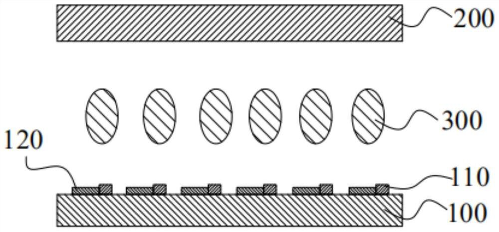
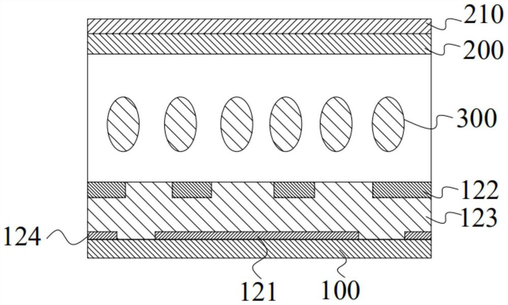
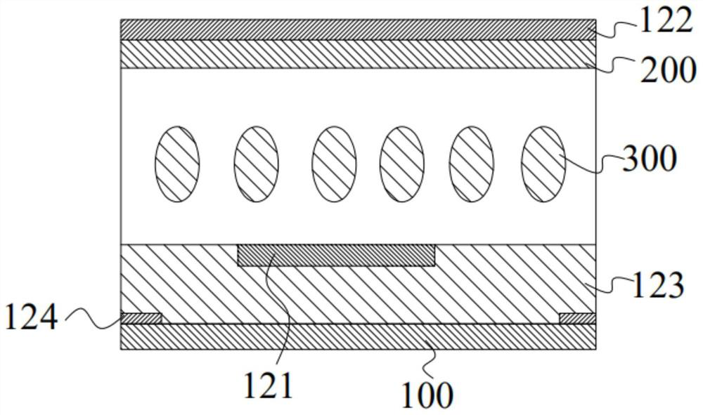
The invention discloses a liquid crystal panel, a display device and a liquid crystal panel manufacturing method. The liquid crystal panel comprises a first substrate, a second substrate and a liquid crystal molecular layer, the first substrate and the second substrate are oppositely arranged, and the liquid crystal molecular layer is arranged between the first substrate and the second substrate; the first substrate comprises a plurality of polarization structures; the polarization structure comprises a pixel electrode and a common electrode 122; the pixel electrode comprises a plurality of first strip-shaped blocks; the common electrode 122 comprises a plurality of second strip-shaped blocks; and the first substrate further comprises a plurality of metal wire grid structures, the metal wire grid structures are arranged below the common electrode 122, and the metal wire grid structures are connected through metal wires. The pixel electrode and the common electrode 122 which are of a strip-shaped structure are arranged, so that the pixel electrode and the common electrode 122 have the traditional pixel electric control function and also have the polarization effect, a traditional iodine-system polaroid or a dye-system polaroid is replaced, the problem that the light transmittance of the traditional polaroid is low is solved, and the display brightness of the display device is improved.

Description

technical field [0001] The present application relates to the technical field of display devices, in particular to a liquid crystal panel, a display device and a method for manufacturing a liquid crystal panel. Background technique [0002] The statements herein merely provide background information related to the present application and do not necessarily constitute exemplary techniques. [0003] Liquid crystal display (LCD for short) is a kind of flat display device, and the polarizing structure is the core component of the liquid crystal display device; in the polarizing structure, most of the iodine type (Iodine type) or dye system ( Dye type) polarizer is used as a polarizing component. The principle of iodine-based or dye-based polarizers is that, in the incident light, the light whose electric field vibration direction is parallel to the long axis of the molecule will be absorbed by the molecule, and the light perpendicular to the long axis of the molecule will be abs...

Claims


Application Information

Patent Timeline
IPC IPC(8): G02F1/1343G02F1/1335G02F1/1333
CPCG02F1/134309G02F1/133528G02F1/1333
Inventor 韩甲伟康报虹
Owner MIANYANG HKC OPTOELECTRONICS TECH CO LTD
Learn More