A vertically integrated unit light emitting diode

A technology of light-emitting diodes and integrated units, applied in electrical components, semiconductor devices, nanotechnology, etc., can solve the problems of LED light efficiency, heat dissipation and stability limitations, and achieve improved light extraction efficiency, large heat dissipation area, and increased effective light output area effect

Active Publication Date: 2022-07-05
纳微朗科技(深圳)有限公司
View PDF7 Cites 0 Cited by
  • Summary
  • Abstract
  • Description
  • Claims
  • Application Information

AI Technical Summary

Problems solved by technology

Therefore, LED light efficiency, heat dissipation and stability under high current will be severely limited

Method used


Image

  • A vertically integrated unit light emitting diode
  • A vertically integrated unit light emitting diode
  • A vertically integrated unit light emitting diode

Examples


Embodiment 1

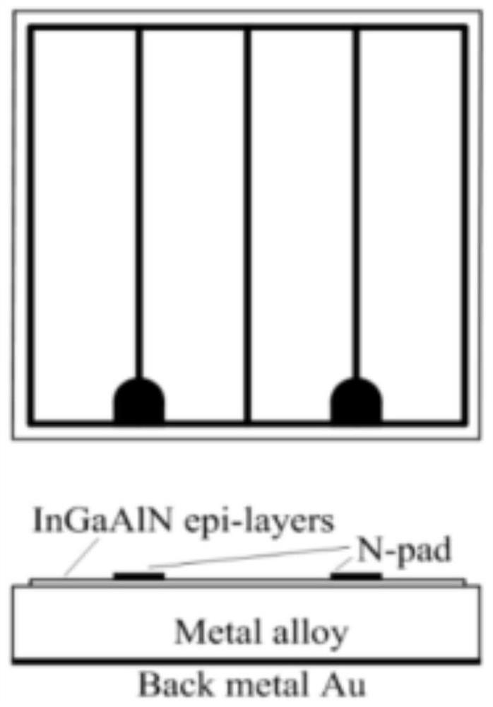
[0060] This embodiment provides a vertically integrated unit light emitting diode, including: a second conductivity type electrode 1, an integral mesa structure 6 composed of a diode unit mesa structure, a trench 7 and a diode unit 8, a second conductivity type electrode line 9, a pad 11. The second conductive type electrode 1 is an N-type conductive electrode. The width of the trench is 0.1 micron and the depth is 0.01 micron, the trench is located between the diode units, and there are linear electrode lines laid in the trench. The N-type conductive electrode is in ohmic contact with the top of the diode unit and is connected to the pad through a bar-shaped electrode line. The number of pads is 1, and the shape is an irregular polygon with an arc edge, which is located on the short edge of the mesa structure. The pads are 0.1 microns thick and 50 microns wide.

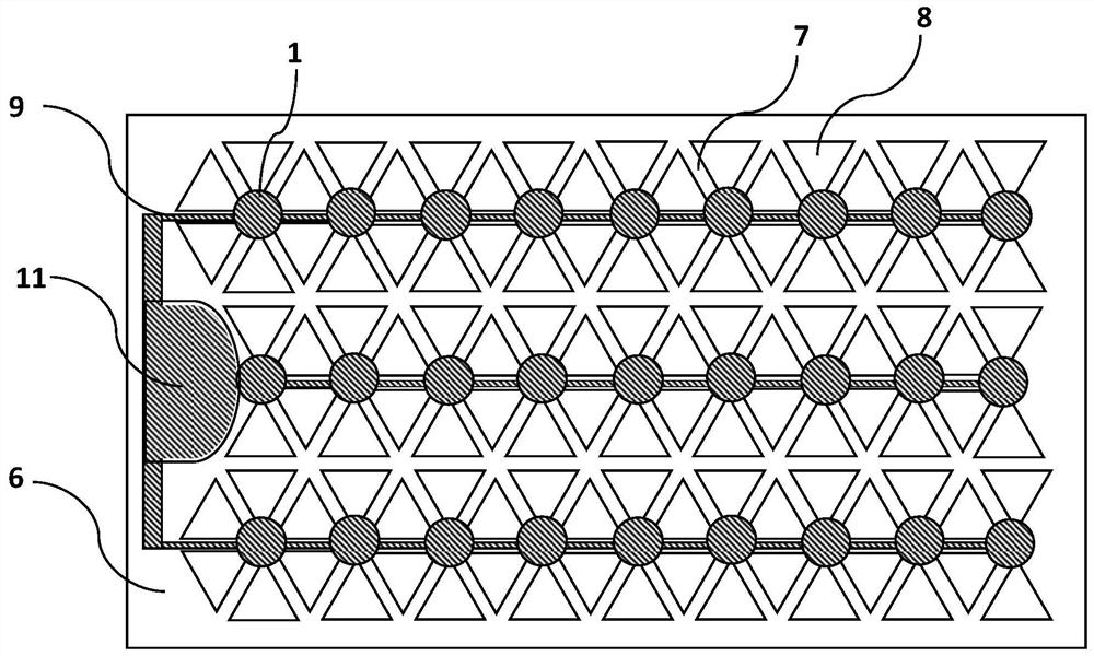
[0061] like image 3 As shown, the overall mesa structure includes 6 rows of 102 triangular diode unit mesas of...

Embodiment 2

[0068] This embodiment provides a vertically integrated unit light emitting diode, such as Figure 8 As shown, it includes: a second conductive type electrode 1, an overall mesa structure 6, a trench 7, a diode unit 8, a second conductive type electrode line 9 and a pad 11, and the second conductive type electrode 1 is an N-type conductive electrode. The trench has a width of 1 micron and a depth of 0.1 micron. The trench structure is located between the diode units. Linear electrode lines are laid in the trench. The electrode lines have a width of 0.1 to 1 micron and a thickness of 0.1 to 1 micron. The N-type conductive electrode is in ohmic contact with the top of the diode unit and is connected to the pad through a bar-shaped electrode line. The number of pads is 1, the shape is a rectangle with rounded corners, located in the middle of the mesa, the thickness of the pad is 1 micron, and the width is 5 microns.

[0069] The chip includes a total of 52 diode units in 6 rows...


PUM

PropertyMeasurementUnit
lengthaaaaaaaaaa
thicknessaaaaaaaaaa
widthaaaaaaaaaa

Abstract

The present invention provides a vertically integrated unit light emitting diode, comprising: forming n diode mesa structures and trench structures on a side away from a first conductivity type electrode, the second conductivity type electrode line along the second conductivity type layer The trenches on the upper part extend, and the distance between adjacent diode units perpendicular to the extending direction of the second conductive type electrode line is determined according to the current diffusion length; the n diode units include a current blocking layer and a protective metal layer, and the protective metal layer A mirror is arranged in the layer, and the current blocking layer is embedded in the protective metal layer and the mirror. The invention effectively blocks the current diffusion in the vertical direction, and the unit diode is designed with a high degree of freedom geometry optimization and a sufficiently small micro-nano structure to promote the lateral diffusion of the current and solve the uneven luminescence caused by the uneven current diffusion. The problem is that the photoelectric conversion efficiency / lumen efficiency is improved.

Description

technical field [0001] The present invention relates to the field of semiconductor materials and device technology, in particular to semiconductor optoelectronic devices, and more particularly, to a vertically integrated unit light emitting diode. Background technique [0002] In the conventional vertical structure LED chip, the current diffusion mainly depends on the N-type conductive electrode side, and there are electrode lead-type leads or drill-type leads, but the overall current diffusion is still uneven, resulting in the loss of luminous efficiency and uneven heat dissipation. Affects the efficiency and stability of the unit diode chip. This limits the vertical high-power LED chips to provide products with higher lumen output per unit area. Uneven current spreading, uneven heat spreading, and uneven light extraction lead to great limitations in three important parameters: lumen efficiency, lumen density output, and lumen cost. The vertical LED chip technology current...

Claims


Application Information

Patent Timeline
Patent Type & Authority Patents(China)
IPC IPC(8): H01L33/38H01L33/14H01L33/20H01L33/64H01L33/10H01L27/15B82Y40/00
CPCH01L33/145H01L33/38H01L33/20H01L33/10H01L33/642H01L33/385H01L27/156B82Y40/00
Inventor 闫春辉蒋振宇
Owner 纳微朗科技(深圳)有限公司
Why Eureka
Try Eureka