Display panel and preparation method thereof and display device

A display panel and display substrate technology, which is applied in semiconductor/solid-state device manufacturing, optics, instruments, etc., to achieve the effect of improving poor viewing angle and color shift

Inactive Publication Date: 2021-06-25
SHENZHEN CHINA STAR OPTOELECTRONICS SEMICON DISPLAY TECH CO LTD
View PDF6 Cites 2 Cited by
  • Summary
  • Abstract
  • Description
  • Claims
  • Application Information

AI Technical Summary

Problems solved by technology

[0005] One of the purposes of the present application is to provide a display panel and its preparation method. A light distribution layer is added to the light-emitting side of the display substrate, and a microlens is fabricated by photolithography, which can not only meet mass production requirements, but also effectively Solve the problems of viewing angle, brightness and color cast of the display panel
[0006] Another object of the present application is to provide a display device. By adding a light distribution layer on the light-emitting side of the display substrate and forming micro-lenses by photolithography, the mass production can be improved, and the viewing angle, brightness and problems of the display panel can be effectively solved. Color shift and other problems

Method used


Image

  • Display panel and preparation method thereof and display device
  • Display panel and preparation method thereof and display device
  • Display panel and preparation method thereof and display device

Examples


Embodiment Construction

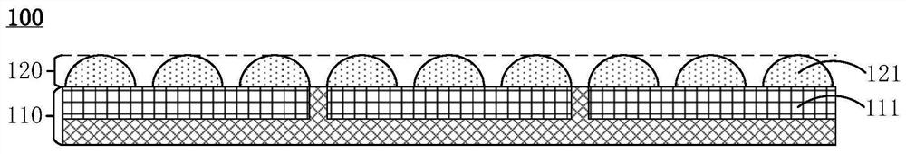
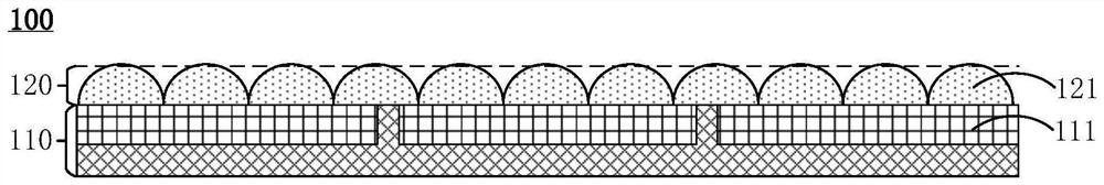
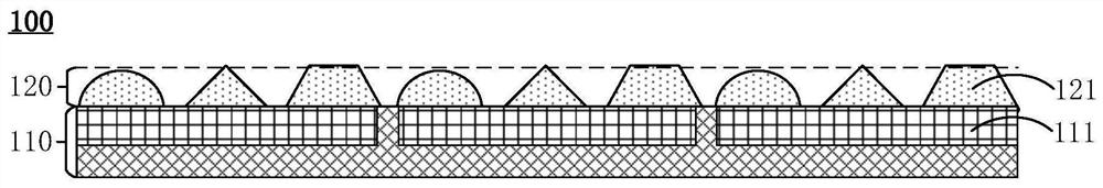
[0027] The following will clearly and completely describe the technical solutions in the embodiments of the application with reference to the drawings in the embodiments of the application. Apparently, the described embodiments are only some of the embodiments of the application, not all of them. Based on the embodiments in this application, all other embodiments obtained by those skilled in the art without making creative efforts belong to the scope of protection of this application. In addition, it should be understood that the specific implementations described here are only used to illustrate and explain the present application, and are not intended to limit the present application. In this application, unless stated otherwise, the used orientation words such as "up", "down", "left" and "right" may refer to the direction of the actual use or working state of the device, or refer to the The drawing direction in the figure may also refer to two opposite directions; while "in...


PUM


Abstract

The invention aims to provide a display panel and a preparation method thereof and a display device. The display panel comprises: a display substrate, wherein the display substrate comprises a plurality of pixel units, and each pixel unit is provided with a light emitting side; and a light distribution layer arranged on the display substrate and located on the light emitting sides of the pixel units, wherein the light distribution layer comprises a plurality of lenses, the lenses correspond to the pixel units, and the orthographic projection area of each lens on the display substrate is smaller than the area of the corresponding pixel unit. According to the display panel, the light distribution layer is additionally arranged on the light emitting side of the display substrate, and the technical scheme that the micro lens is achieved through the photoetching method is adopted, so that the requirement for mass production can be met, and the visual angle, the brightness, the color cast and the like of the display panel can be effectively improved.

Description

technical field [0001] The present application relates to the field of display technology, in particular to a display panel, a manufacturing method thereof, and a display device using the display panel. Background technique [0002] OLED display panel (Organic Light Emitting Display) has self-illumination, no backlight, high contrast, thin thickness, wide viewing angle, fast response speed, can be used for flexible panels, wide operating temperature range, and relatively simple structure and manufacturing process And other excellent characteristics, it is considered to be an emerging application technology of the next generation of flat panel display devices. But it also has some defects of its own. On the one hand, the brightness of OLED is low, and its stability is slightly worse than other displays; It is because of the microcavity effect of the R / G / B pixel light-emitting device in the inkjet printed OLED display panel. [0003] In order to improve the viewing angle and...

Claims


Application Information

Patent Timeline
Patent Type & Authority Applications(China)
IPC IPC(8): H01L51/52H01L51/56H01L27/32H01L33/58H01L27/15G02F1/1335
CPCH01L33/58H01L27/156G02F1/133526H01L2933/0058H10K59/12H10K50/858H10K59/1201H10K71/00
Inventor 陈黎暄
Owner SHENZHEN CHINA STAR OPTOELECTRONICS SEMICON DISPLAY TECH CO LTD
Why Eureka
Try Eureka