A kind of reactive ion etching device and method for continuously preparing large-area nano textured surface

A technology of reactive ion etching and nano suede, which is applied in the direction of nanotechnology, sustainable manufacturing/processing, transportation and packaging, etc., can solve the problems of low production capacity and large surface damage, so as to improve production capacity, ensure rapid continuity, The effect of continuous dynamic etching

Active Publication Date: 2022-03-22
JIANGSU UNIV +2
View PDF15 Cites 0 Cited by
  • Summary
  • Abstract
  • Description
  • Claims
  • Application Information

AI Technical Summary

Problems solved by technology

[0010] The technical problem to be solved by the present invention is: how to overcome the problems of low production capacity and large surface damage caused by the etching process of the existing reactive ion etching technology, further improve the etching production capacity, reduce the etching damage, and provide a continuous preparation of large-area Reactive ion etching device for nanotexture

Method used


Image

  • A kind of reactive ion etching device and method for continuously preparing large-area nano textured surface
  • A kind of reactive ion etching device and method for continuously preparing large-area nano textured surface
  • A kind of reactive ion etching device and method for continuously preparing large-area nano textured surface

Examples


Embodiment 1

[0061] 1. Clean and pretreat the pre-fabricated silicon wafer to obtain the damaged silicon wafer.

[0062] 2. Put the damaged silicon wafer on the carrier plate of the loading table, and the carrier plate is driven by the transmission rollers into the process chamber through the loading chamber and the process buffer chamber in turn;

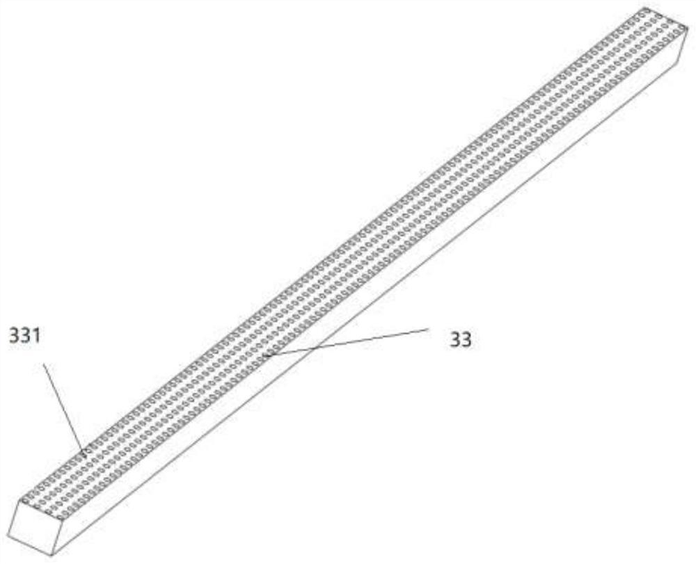
[0063] 3. Turn on the vacuuming equipment, press the air pressure until the predetermined vacuum value is 1Pa, and feed SF from the process air intake equipment 6 , O 2 and SiCl 4 Etching gas, the gas flow rate is 1900sccm, 3000sccm and 1500sccm respectively, turn on the magnetic field device, the etching gas enters the process chamber uniformly from the linear ion source distribution holes, and maintain the process chamber pressure at 24Pa.

[0064] 4. Turn on the radio frequency power supply, turn on the magnetic field device, the power of the high frequency power supply is 1950W, and the power of the low frequency power supply is 750W. The...

Embodiment 2

[0069] 1. Clean and pre-treat the pre-fabricated silicon wafers to obtain the damaged silicon wafers;

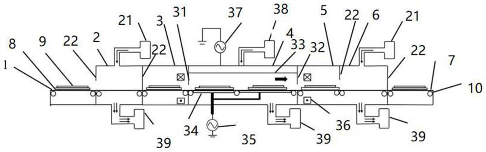
[0070] 2. Put the damaged silicon wafer on the carrier plate of the loading table of the reactive ion etching equipment. The reactive ion etching equipment such as figure 1 As shown, it includes a loading table, a loading chamber, a process buffer chamber, a process chamber, an unloading buffer chamber, an unloading chamber, an unloading table, a base, and a conveying system. Driven by the transmission rollers, the carrier board passes through the loading chamber and the process buffer chamber of the reaction ion equipment in turn, and enters the process chamber;

[0071] 3. Turn on the vacuuming equipment until the predetermined vacuum value is 0.5Pa, and enter the SF from the process air intake equipment 6 , O 2 and SiCl 4 For etching gas, the gas flow rates are 1850sccm, 2900sccm and 1650sccm respectively. The magnetic field device is turned on, and the etching gas ent...


PUM

PropertyMeasurementUnit
reflectanceaaaaaaaaaa

Abstract

The invention relates to a reactive ion etching method for continuously preparing a large-area nano-textured surface, comprising S1: cleaning and pretreating a pre-textured silicon chip; S2: placing the damaged silicon chip on a carrier plate of a loading platform After that, enter the process chamber through the loading chamber and the process buffer chamber in turn; S3: open the vacuum equipment, SF 6 , O 2 and SiCl 4 Etching gas enters the process chamber uniformly from the linear ion source distribution holes; S4: Turn on the radio frequency power supply and magnetic field device, and the etching gas is ionized to generate plasma; under the action of the electric field, the high-energy ions shoot vertically to the sample surface for physical bombardment, and the process is completed. Etching of the silicon wafer in the process chamber; S5: The silicon wafer passes through the unloading buffer chamber and the unloading chamber sequentially from the process chamber along with the carrier, and is finally taken out to the unloading table. The invention combines a plurality of large-size linear ion sources to realize large-area uniform etching. Continuous dynamic etching of silicon wafers can be realized through the synergistic effect of loading chamber, unloading chamber and conveying mechanism, which greatly improves the production capacity of RIE.

Description

technical field [0001] The invention relates to the technical field of solar nano-velvet production, in particular to a reactive ion etching device and method for continuously preparing large-area nano-velvet. Background technique [0002] In the manufacturing process of crystalline silicon solar cells, in order to reduce the surface reflectance of silicon wafers and reduce light loss, the surface of silicon wafers is often textured to form a micro-nano light-trapping structure on the surface, commonly known as "texturing". ". In the prior art, due to the strong anisotropy and high etching selection ratio of the RIE texture making process, nano-scale texture (less than 1um) can be produced to form a texture structure with low reflectivity, while As an important method for texturing the surface of silicon wafers. However, during the RIE texturing process, ions bombard the surface of the silicon wafer under the action of self-bias for etching, which will also cause a certain...

Claims


Application Information

Patent Timeline
Patent Type & Authority Patents(China)
IPC IPC(8): H01L21/677H01L31/18H01L21/3065H01L31/0236H01J37/20H01J37/305B82Y40/00
CPCH01L31/1804H01L31/02363H01L21/3065H01L31/1876H01L21/67742H01L21/6776H01J37/3056H01J37/20B82Y40/00Y02P70/50
Inventor 丁建宁孙涛李绿洲上官泉元
Owner JIANGSU UNIV
Why Eureka
Try Eureka