Method for preventing layer staggering in lamination of multi-layer circuit board

A multi-layer circuit, error-proofing technology, applied in the direction of multi-layer circuit manufacturing, printed circuit, printed circuit manufacturing, etc., can solve the problems of high labor intensity and high scrap rate, reduce labor intensity, reduce scrap rate and high accuracy Effect

Inactive Publication Date: 2021-07-09
AOSHIKANG TECH CO LTD
View PDF4 Cites 0 Cited by
  • Summary
  • Abstract
  • Description
  • Claims
  • Application Information

AI Technical Summary

Problems solved by technology

In the process of PCB board processing, multi-layer PCB core boards need to be superimposed and hot-melted. When the existing method is hot-melt matching, the personnel visually confirm the number of inner board side layers. This operation has misplaced and reversed. , Put more, less put the core board risk, resulting in high scrap rate, high labor intensity of workers

Method used


Image

  • Method for preventing layer staggering in lamination of multi-layer circuit board
  • Method for preventing layer staggering in lamination of multi-layer circuit board
  • Method for preventing layer staggering in lamination of multi-layer circuit board

Examples


no. 1 example

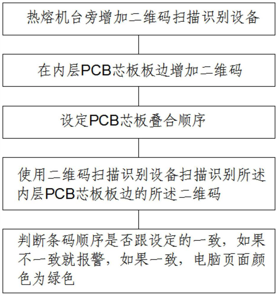
[0028] Please refer to figure 1 , in the first embodiment of the present invention, the method for laminating the error prevention layer of a multilayer circuit board includes the following steps:

[0029] S1: Add a QR code scanning recognition device next to the hot-melt machine;

[0030] S2: Add a QR code on the edge of the inner PCB core board;

[0031] S3: Set the stacking sequence of PCB core boards;

[0032] S4: Use a two-dimensional code scanning recognition device to scan and identify the two-dimensional code on the edge of the inner PCB core board;

[0033] S5: Judging whether the barcode sequence is consistent with the setting, if not, it will alarm, if it is consistent, the color of the computer page is green.

[0034] The two-dimensional code scanning recognition device is connected to a computer, and the two-dimensional code scanning recognition device is adapted to the software in the computer.

[0035] The two-dimensional code information includes the materi...

no. 2 example

[0043] Based on the method for laminating an anti-error layer on a multilayer circuit board provided in the first embodiment of the present application, the second embodiment of the present application proposes another method for laminating an anti-error layer on a multilayer circuit board. The second embodiment is only a preferred mode of the first embodiment, and the implementation of the second embodiment will not affect the independent implementation of the first embodiment.

[0044] The second embodiment of the present invention will be further described below in conjunction with the drawings and implementation methods.

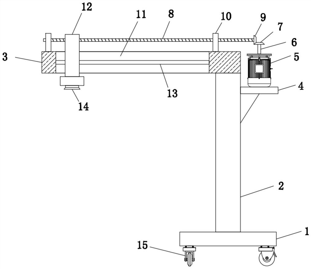
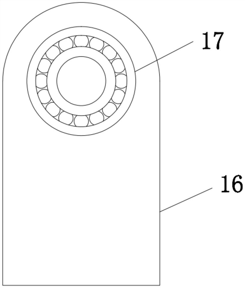
[0045] Please refer to Figure 2-Figure 3 The difference between this embodiment and the first embodiment is that the two-dimensional code scanning recognition device includes a base 1, a column 2 is fixedly installed on the top side of the base 1, and a top plate 3 is fixedly installed on the top side of the column 2 , a lateral moving device is instal...


PUM


Abstract

The invention provides a method for preventing layer staggering in lamination of a multi-layer circuit board. The multilayer circuit board lamination mistake proofing method comprises the following steps: S1, adding a QR code scanning identification device beside a hot melting machine; S2, adding a QR code to the board edge of the inner-layer PCB core board; S3, setting a stacking sequence of the PCB core boards; S4, scanning and identifying the QR code on the board edge of the inner-layer PCB core board by using QR code scanning and identifying equipment; S5, judging whether the sequence of the bar codes is consistent with the set sequence: if not, alarming, and if so, determining that the color of the computer page is green. The multilayer circuit board lamination mistake-proofing method provided by the invention has the advantages of high accuracy, low rejection rate and low labor intensity of workers.

Description

technical field [0001] The invention relates to the technical field of PCB board processing, in particular to a method for laminating anti-error layers of multilayer circuit boards. Background technique [0002] PCB board, also known as printed circuit board, is the provider of electrical connection for electronic components. In the process of PCB board processing, multi-layer PCB core boards need to be superimposed and hot-melted. When the existing method is hot-melt matching, the personnel visually confirm the number of inner board side layers. This operation has misplaced and reversed. , Put more, less risk of putting core boards, resulting in high scrap rate and high labor intensity of workers. [0003] Therefore, it is necessary to provide a new method for laminating the anti-error layer of a multilayer circuit board to solve the above technical problems. Contents of the invention [0004] The technical problem to be solved by the invention is to provide a method fo...

Claims


Application Information

Patent Timeline
Patent Type & Authority Applications(China)
IPC IPC(8): H05K3/46
CPCH05K3/4644
Inventor 孟伟
Owner AOSHIKANG TECH CO LTD
Why Eureka
Try Eureka