Display panel, manufacturing method thereof and display device

A technology for display panels and substrates, applied in semiconductor/solid-state device manufacturing, semiconductor devices, electrical components, etc., can solve problems such as poor display effect, and achieve effective overlap, increase overlap area, and improve display effect.

Active Publication Date: 2021-07-16
HEFEI XINSHENG OPTOELECTRONICS TECH CO LTD +1
View PDF19 Cites 4 Cited by
  • Summary
  • Abstract
  • Description
  • Claims
  • Application Information

AI Technical Summary

Problems solved by technology

The problem of poor display effect of OLED display panels in the prior art can be solved, and the technical solution is as follows:

Method used


Image

  • Display panel, manufacturing method thereof and display device
  • Display panel, manufacturing method thereof and display device
  • Display panel, manufacturing method thereof and display device

Examples


Embodiment Construction

[0045] In order to make the purpose, technical solution and advantages of the present application clearer, the implementation manners of the present application will be further described in detail below in conjunction with the accompanying drawings.

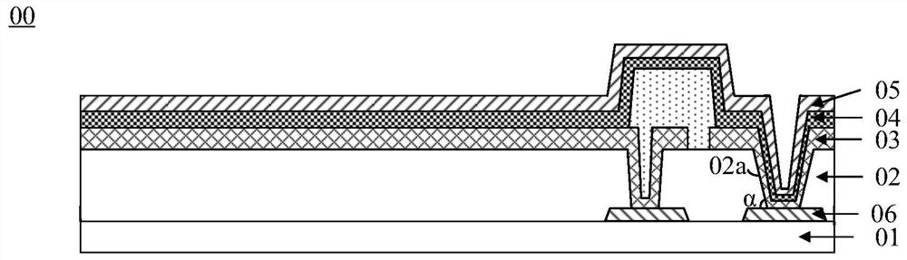
[0046] In related art, please refer to figure 1 , figure 1 It is a structural schematic diagram of a display panel provided by the related art. The display panel 00 may include:

[0047] Substrate 01.

[0048] An insulating layer 02 located on a substrate 01 , and an auxiliary electrode 03 , a light emitting layer 04 and a cathode layer 05 which are stacked in sequence.

[0049] The insulating layer 02 has a via hole 02a. The light-emitting layer 04 may be disconnected in the via hole 02a, so that the auxiliary electrode 03 and the cathode layer 05 can be overlapped in the via hole 02a.

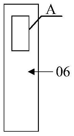
[0050] Please refer to figure 1 and figure 2 , figure 2 Yes figure 1 A partial top view of the display panel shown. The display pan...


PUM

PropertyMeasurementUnit
thicknessaaaaaaaaaa

Abstract

The invention discloses a display panel, a manufacturing method thereof and a display device, and belongs to the technical field of display. The display panel comprises a substrate, an insulating layer, an auxiliary electrode, a light-emitting layer and a cathode layer. The auxiliary electrode and the cathode layer are in lap joint through a first via hole in the insulating layer, and the opening of the first via hole is polygonal, so that a broken line is formed at each edge of the opening of the light-emitting layer, the light-emitting layer is not attached to each side wall of the auxiliary electrode in the first via hole, the lap joint area of the auxiliary electrode and the cathode layer is increased, effective lap joint between the cathode layer and the auxiliary electrode is achieved, and the display effect of the display panel is improved.

Description

technical field [0001] The present application relates to the field of display technology, in particular to a display panel, a manufacturing method thereof, and a display device. Background technique [0002] The current organic electroluminescent (English: Organic Light-Emitting Diode abbreviation: OLED) display panel usually includes an anode layer, an organic light-emitting layer and a cathode layer, which can be divided into bottom-emitting OLED display panels and top-emitting OLEDs according to different light-emitting surfaces. There are two types of display panels. Since the top-emitting OLED display panel can obtain a larger aperture ratio, it has become a research hotspot in recent years. [0003] A top-emission OLED display panel requires a thin and transparent cathode layer and an anode layer capable of light reflection to increase light transmittance. However, the thin and transparent cathode layer generally has the problems of high resistance value and serious...

Claims


Application Information

Patent Timeline
Patent Type & Authority Applications(China)
IPC IPC(8): H01L51/52H01L51/56H01L27/32
CPCH10K59/12H10K50/824H10K59/1201H10K71/00
Inventor 刘宁王庆贺刘军尹浩周斌闫梁臣
Owner HEFEI XINSHENG OPTOELECTRONICS TECH CO LTD
Why Eureka
Try Eureka