Black welding strip for photovoltaic module and processing method of black welding strip
A technology of photovoltaic modules and processing methods, applied in photovoltaic power generation, laser welding equipment, metal processing equipment, etc., can solve problems such as limiting production efficiency, reducing curing time, and unable to increase curing temperature, so as to reduce production costs and improve production efficiency. , the effect of saving production steps and time
- Summary
- Abstract
- Description
- Claims
- Application Information
AI Technical Summary
Problems solved by technology
Method used
Image

Examples
Embodiment 2
[0024] Embodiment 2: a kind of processing method of black welding strip, mainly comprises the following steps:
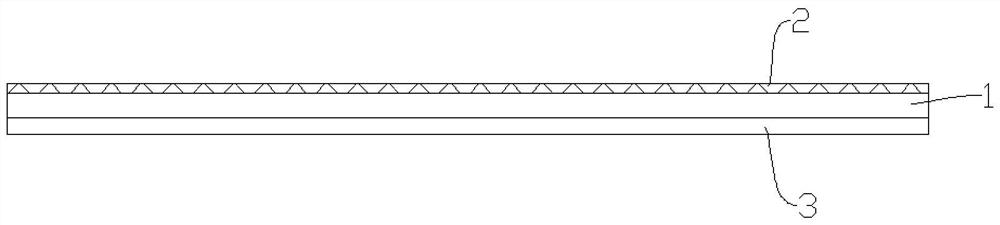
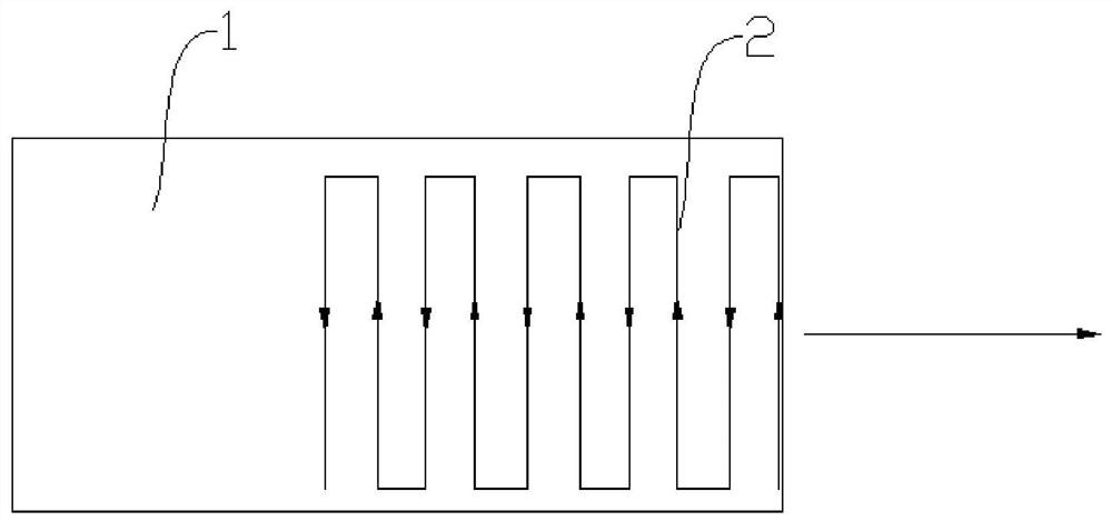
[0025] Formation of the black etching layer 2: use a nanosecond laser to perform laser etching on the exposed surface of the copper base layer 1, such as figure 2 As shown, the nanosecond laser performs reciprocating scanning and etching perpendicular to the production movement direction of the copper base layer 1, thereby forming a black etching layer 2 on the exposed surface of the other side of the copper base layer 1. The black etching layer 2 is a microstructure, and the light is in The surface of the microstructure refracts and absorbs to form a black visual effect.
[0026] During etching, the distance between the laser emitting end of the nanosecond laser and the exposed surface on one side of the copper base layer 1 is 10 cm, the reciprocating speed of the nanosecond laser is 200 mm / s, and the production speed of the copper base layer 1 is 5 m / min. Becaus...
Embodiment 3
[0033] Embodiment 3: a kind of processing method of black welding strip, mainly comprises the following steps:
[0034] Formation of the black etching layer 2: use a nanosecond laser to perform laser etching on the exposed surface of the copper base layer 1, such as figure 2 As shown, the nanosecond laser performs reciprocating scanning and etching perpendicular to the production movement direction of the copper base layer 1, thereby forming a black etching layer 2 on the exposed surface of the other side of the copper base layer 1. The black etching layer 2 is a microstructure, and the light is in The surface of the microstructure refracts and absorbs to form a black visual effect.
[0035] During etching, the distance between the laser emitting end of the nanosecond laser and the exposed surface on one side of the copper base layer 1 is 15 cm, the reciprocating speed of the nanosecond laser is 350 mm / s, and the production speed of the copper base layer 1 is 7 m / min. Becaus...
Embodiment 4
[0042] Embodiment 4: a kind of processing method of black welding strip, mainly comprises the following steps:
[0043] Formation of the black etching layer 2: use a nanosecond laser to perform laser etching on the exposed surface of the copper base layer 1, such as figure 2 As shown, the nanosecond laser performs reciprocating scanning and etching perpendicular to the production movement direction of the copper base layer 1, thereby forming a black etching layer 2 on the exposed surface of the other side of the copper base layer 1. The black etching layer 2 is a microstructure, and the light is in The surface of the microstructure refracts and absorbs to form a black visual effect.
[0044] During etching, the distance between the laser emitting end of the nanosecond laser and the exposed surface on one side of the copper base layer is 20 cm, the reciprocating speed of the nanosecond laser is 500 mm / s, and the production speed of the copper base layer 1 is 10 m / min. Because...
PUM
| Property | Measurement | Unit |
|---|---|---|
| wavelength | aaaaa | aaaaa |
Abstract
Description
Claims
Application Information
 - R&D Engineer
- R&D Manager
- IP Professional
- Industry Leading Data Capabilities
- Powerful AI technology
- Patent DNA Extraction
Browse by: Latest US Patents, China's latest patents, Technical Efficacy Thesaurus, Application Domain, Technology Topic.
© 2024 PatSnap. All rights reserved.Legal|Privacy policy|Modern Slavery Act Transparency Statement|Sitemap