
Display panel, preparation method thereof and display device

A display panel and surface structure technology, applied in semiconductor/solid-state device manufacturing, electrical components, electric solid-state devices, etc., can solve problems such as high production costs, printing ink material consumption, and high printing accuracy requirements

Pending Publication Date: 2021-07-30
SHENZHEN CHINA STAR OPTOELECTRONICS SEMICON DISPLAY TECH CO LTD
View PDF7 Cites 0 Cited by
  • Summary
  • Abstract
  • Description
  • Claims
  • Application Information

AI Technical Summary

Problems solved by technology

[0003] At present, OLED devices are mainly prepared by evaporation or inkjet printing, but evaporation faces problems such as mask (mask) deformation, substrate film wear, low material utilization rate, and high equipment investment in large-scale applications. Therefore, the current The development trend is to adopt the process of inkjet printing
In inkjet printing OLED, there are two main structural designs for pixels: one is the red, green and blue sub-pixel unit SBS (Side by Side, arranged side by side) pixel arrangement design, this design consumes less ink, but It requires high equipment precision, easy to mix colors, and has a large yield loss; the other is the Line-Bank (linear bank) pixel arrangement design, which is to print a whole line of sub-pixels of the same color in the same Bank area, that is, Red, green and blue three-color sub-pixel units are printed as a whole pixel. This design consumes a lot of organic ink materials on large-sized OLED devices, resulting in high cost
[0004] Therefore, there is a need for a new display panel, its preparation method, and display device to solve the problem of high printing accuracy in the pixel structure design of the existing display panel generated by inkjet printing, resulting in a large yield loss or printing The technical problem of high production cost due to high consumption of ink materials

Method used


Image

  • Display panel, preparation method thereof and display device
  • Display panel, preparation method thereof and display device
  • Display panel, preparation method thereof and display device

Examples


Embodiment 1

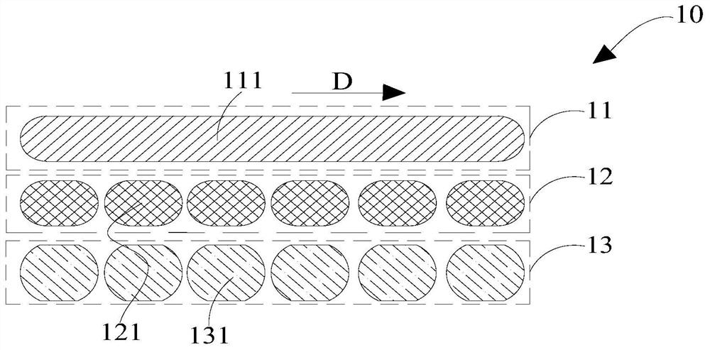
[0036] Such as figure 1 As shown, it is a schematic diagram of the pixel structure of the display panel provided in the first embodiment of the present application; wherein, the display panel includes at least one pixel unit 10, and each of the pixel units 10 includes first sub-pixels 11 with different light emitting colors, The second sub-pixel 12 and the third sub-pixel 13, the first sub-pixel 11, the second sub-pixel 12 and the third sub-pixel 13 are arranged in sequence along the first direction;

[0037] Wherein, the first sub-pixel 11 is a continuous linear structure 111, the third sub-pixel 13 includes a plurality of third sub-pixel blocks 131 arranged at intervals along the second direction D, and the second sub-pixel 12 includes A plurality of second sub-pixel blocks 121 arranged at intervals in a second direction D, where the second direction D is perpendicular to the first direction.

[0038] Optionally, in this embodiment of the present application, the light emit...

Embodiment 2

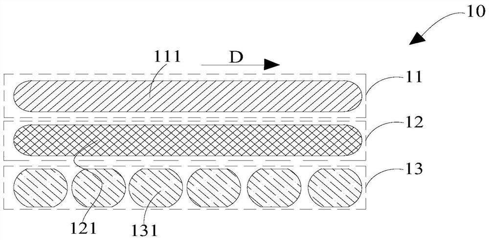
[0048] Such as figure 2 As shown, it is a schematic diagram of the pixel structure of the display panel provided by the second embodiment of the present application; wherein, the difference between the second embodiment of the present application and the first embodiment of the present application is only that:

[0049] The first sub-pixel 11 is a continuous linear structure 111, the second sub-pixel 12 is a continuous linear structure 121, and the third sub-pixel 13 includes a plurality of third sub-pixel blocks arranged at intervals along the second direction 131.

[0050] Optionally, in this embodiment of the present application, the light emitting color of the first sub-pixel 11 is red, the light emitting color of the second sub-pixel 12 is green, and the light emitting color of the third sub-pixel 13 is blue .

Embodiment 3

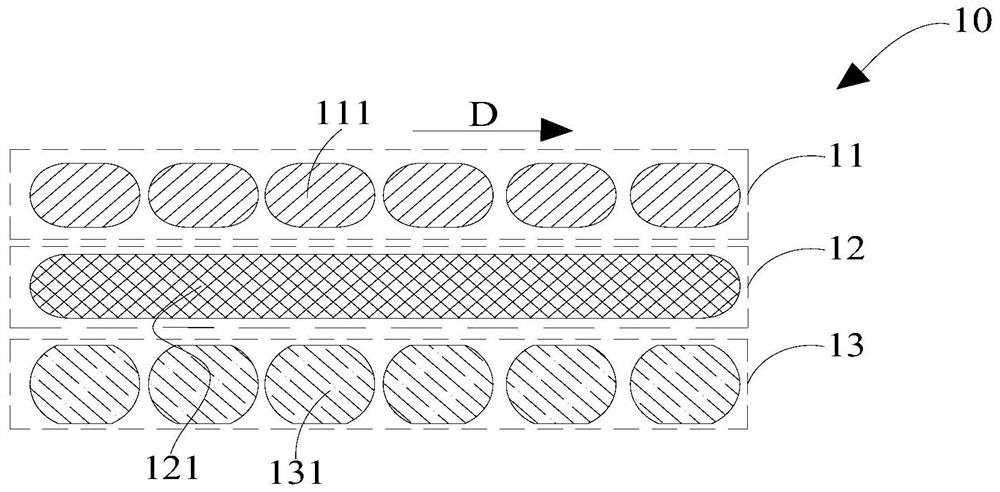
[0052] Such as image 3 As shown, it is a schematic diagram of the pixel structure of the display panel provided by the third embodiment of the present application; where, the difference between the third embodiment of the present application and the first embodiment of the present application is only that:

[0053] The first sub-pixel 11 includes a plurality of first sub-pixel blocks 111 arranged at intervals along the second direction D, and the third sub-pixel 13 includes a plurality of third sub-pixel blocks 131 arranged at intervals along the second direction D, The second sub-pixel 12 is a continuous linear structure 121 .

[0054] Optionally, in this embodiment of the present application, the light emitting color of the first sub-pixel 11 is red, the light emitting color of the second sub-pixel 12 is green, and the light emitting color of the third sub-pixel 13 is blue .


PUM


Abstract

The embodiment of the invention provides a display panel, a preparation method thereof and a display device. The display panel comprises at least one pixel unit; each pixel unit comprises a first sub-pixel, a second sub-pixel and a third sub-pixel which emit light of different colors; the first sub-pixel, the second sub-pixel and the third sub-pixel are sequentially arranged in a first direction; and the first sub-pixel is of a continuous linear structure, the third sub-pixel comprises a plurality of third sub-pixel blocks arranged at intervals in a second direction, the second sub-pixel is of a continuous linear structure or comprises a plurality of second sub-pixel blocks arranged at intervals in the second direction, and the second direction is perpendicular to the first direction. According to the embodiment of the invention, the requirement on printing precision can be reduced while the demand for organic ink is reduced.

Description

technical field [0001] The present application relates to the field of display technology, in particular to a display panel, a manufacturing method thereof, and a display device. Background technique [0002] In terms of display, OLED (Organic Light Emitting Diode, Organic Light Emitting Diode) devices have high contrast, fast response speed, no backlight and are thinner, and can meet consumers' future needs in terms of flexible product forms. Currently showing the mainstream development direction. [0003] At present, OLED devices are mainly prepared by evaporation or inkjet printing, but evaporation faces problems such as mask (mask) deformation, substrate film wear, low material utilization rate, and high equipment investment in large-scale applications. Therefore, the current The development trend is to adopt the process of inkjet printing. In inkjet printing OLED, there are two main structural designs for pixels: one is the red, green and blue sub-pixel unit SBS (Side...

Claims


Application Information

Patent Timeline
IPC IPC(8): H01L27/32H01L21/77
CPCH10K59/35H10K59/352H10K59/353H10K59/121H10K59/1201
Inventor 罗欢周星宇
Owner SHENZHEN CHINA STAR OPTOELECTRONICS SEMICON DISPLAY TECH CO LTD
Learn More