Packaging structure and packaging method of distance sensor
A technology of distance sensor and packaging structure, which is applied in the direction of measuring distance, instruments, measuring devices, etc., can solve the problem of low detection accuracy of distance sensor, achieve the effect of solving low detection accuracy and improving detection accuracy
- Summary
- Abstract
- Description
- Claims
- Application Information
AI Technical Summary
Problems solved by technology
Method used
Image
Examples
Embodiment 1
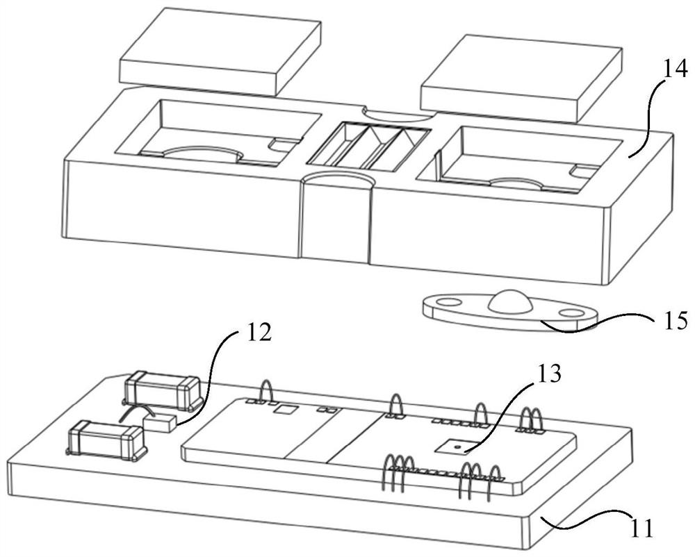
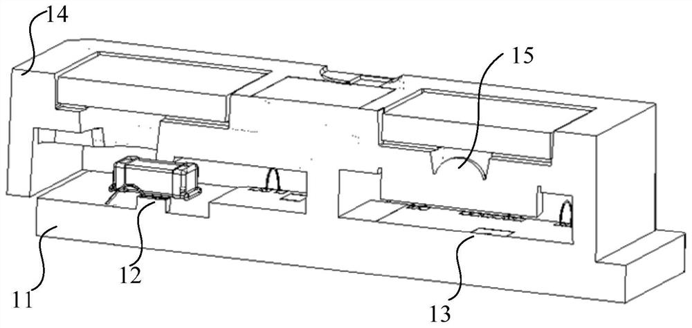
[0065] Please refer to Figure 4 , a package structure of a distance sensor, comprising a substrate 100, a light emitting chip 200, a sensing chip 300, an insulating support 400 and a light-shielding adhesive wall assembly, the light emitting chip 200 and the sensing chip 300 are mounted on the first surface of the substrate 100 at intervals 101, the insulating support 400 is mounted on the first surface 101 of the substrate 100 to cover the light-emitting chip 200 and the sensing chip 300, the insulating support 400 has a first light hole 410 and a second light hole 420, the position of the first light hole 410 is the same as The position of the photosensitive region 310 at the receiving end of the sensing chip 300 corresponds to that of the light-emitting chip 200 , and the position of the second aperture 420 corresponds to that of the light-emitting chip 200 .
[0066] Please refer to Figure 5 , the sensing chip 300 is used for sensing the light source emitted by the ligh...
Embodiment 2
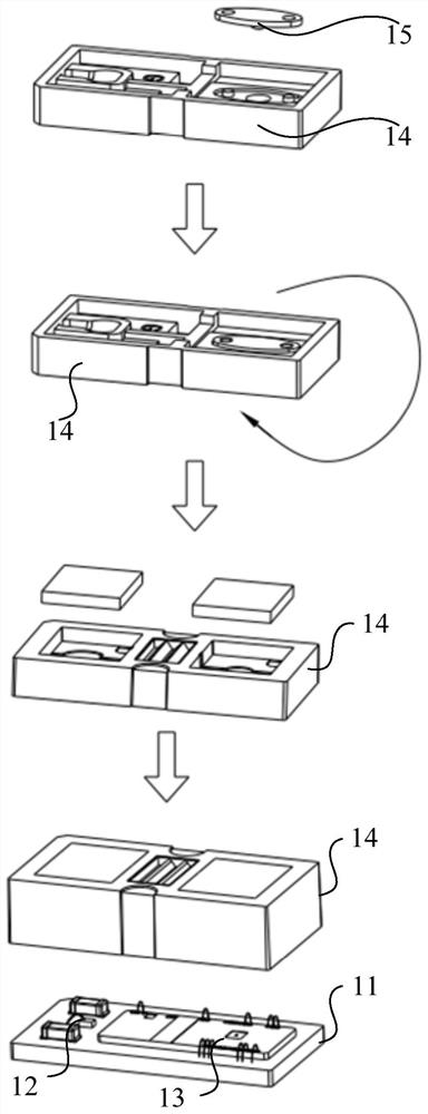
[0088] The invention provides a method for packaging a distance sensor, comprising the following steps:
[0089] S100 , please refer to FIG. 6( a ), provide a substrate 100 , and mount light emitting chips 200 and sensing chips 300 on the first surface 101 of the substrate 100 at intervals. Optionally, the light emitting chip 200 is electrically connected to the substrate 100 through a wire bonding process. The sensing chip 300 is electrically connected to the substrate 100 through a wire bonding process. In particular, the sensing chip 300 is electrically connected to the substrate 100 through gold wires.
[0090] S200, please refer to FIG. 6(b) and FIG. 6(c), provide an insulating bracket 400 with a first light hole 410 and a second light hole 420, and install the lens 710 and the first filter 720 on the first light hole respectively. The bottom end and the top end of the hole 410 , and the second filter 730 is installed on the top end of the second light hole 420 .
[00...
Embodiment 3
[0120] Please refer to Figure 10 , Embodiment 3 provides a packaging structure of a distance sensor, specifically, the insulating bracket 400 has a glue filling groove 430, and the glue filling groove 430 divides the inner chamber of the insulating bracket 400 into a first chamber and a second chamber, The separation glue wall 600 extends into the glue filling groove 430, and the separation glue wall 600 fills the gap between the glue filling groove 430 and the sensing chip 300 to prevent light leakage in the gap, and the separation glue wall 600 makes the gap between the first chamber and the second chamber The light does not interfere with each other, and the recognition accuracy of the distance sensor is higher.
[0121] Specifically, the top of the separating glue wall 600 is flush with the top of the insulating support 400, and the height of the glue filling groove 430 is smaller than the distance between the sensing chip 300 and the top surface of the insulating support...
PUM
 Abstract
Description
Claims
Application Information
 - R&D
- Intellectual Property
- Life Sciences
- Materials
- Tech Scout
- Unparalleled Data Quality
- Higher Quality Content
- 60% Fewer Hallucinations
Browse by: Latest US Patents, China's latest patents, Technical Efficacy Thesaurus, Application Domain, Technology Topic, Popular Technical Reports.
© 2025 PatSnap. All rights reserved.Legal|Privacy policy|Modern Slavery Act Transparency Statement|Sitemap|About US| Contact US: help@patsnap.com


