

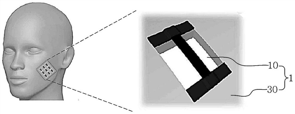
Electronic device attachable to skin and manufacturing method therefor
A technology for electronic devices and skins, which is applied in the manufacture/assembly of piezoelectric/electrostrictive devices, circuits, electrical components, etc., and can solve the problems of difficulty in miniaturization, difficult integration of circuit components, and complicated preparation process.
- Summary
- Abstract
- Description
- Claims
- Application Information
AI Technical Summary
Problems solved by technology
Method used
Image

Examples
no. 1 example
[0119] Figure 4a to Figure 4b A conceptual diagram schematically showing the manufacturing process of the skin sensor according to the first embodiment of the present invention.
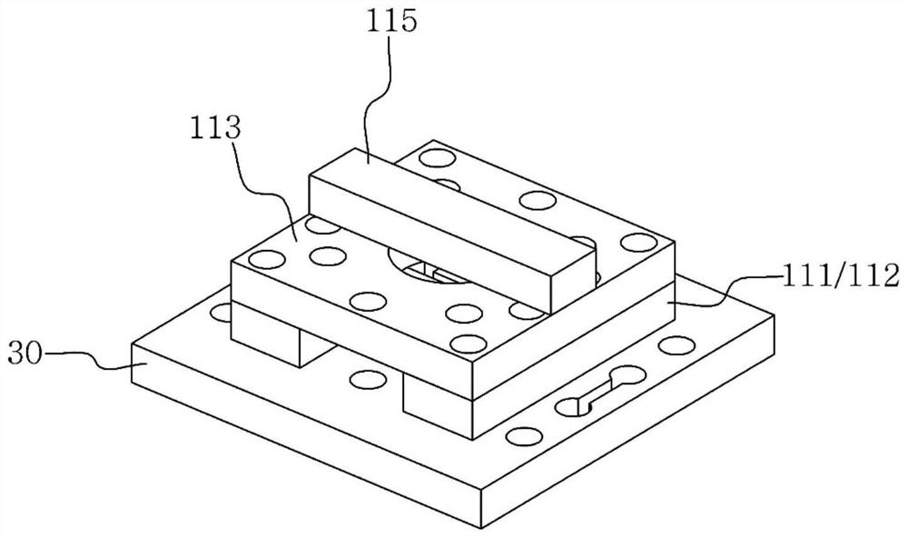
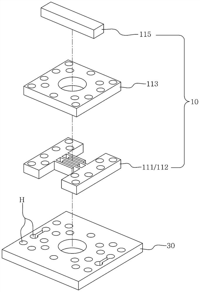
[0120] refer to Figure 4a and Figure 4b The method for preparing the skin sensor 1 according to the first embodiment of the present invention includes the following steps: forming a sacrificial layer 105 on the substrate 101 (step S401); forming the sensor circuit unit 10 on the sacrificial layer 105 (step S410); The sensor circuit unit 10 (that is, the active layer 115) and the flexible patch 30 are bonded (bonding) (step S430); and the sacrificial layer 105 is etched to prepare a skin sensor 1 (step S450 ), wherein, forming the sensor circuit unit 10 on the sacrificial layer 105 (step S410) includes the following steps: forming electrodes 111 and / or interconnectors 112 on the sacrificial layer 105 (step S411); and / or forming an insulating layer 113 on the interconnector (step S413); and formi...
no. 2 example
[0267] Figure 11a to Figure 11b A conceptual diagram schematically showing a manufacturing process of a skin sensor according to a second embodiment of the present invention.
[0268] Referring to FIGS. 4 and 11 , a method of fabricating a skin sensor according to a second embodiment of the present invention is substantially similar to that of the skin sensor according to the first embodiment in FIG. 4 , so differences will be mainly described.
[0269] As shown in FIG. 4 , the active layer 115 of the sensor circuit unit 10 is formed closest to the flexible patch 30 among the components of the sensor circuit unit 10 .
[0270] However, in another embodiment, the active layer 115 of the sensor circuit unit 10 may be formed furthest from the flexible patch 30 among the components of the sensor circuit unit 10 . That is, it is possible to prepare Figure 1b and Figure 1c The skin sensor in 1.
[0271] Similar to the first embodiment, the manufacturing method of the skin-att...
no. 3 example
[0276] Figure 12a to Figure 12h A conceptual diagram schematically showing a manufacturing process of a skin sensor according to a third embodiment of the present invention.
[0277] Referring to FIGS. 4 and 12 , a method of fabricating a skin sensor according to a third embodiment of the present invention is substantially similar to that of the skin sensor according to the first embodiment in FIG. 4 , so differences will be mainly described.
[0278] According to the manufacturing method of the skin sensor of the second embodiment, the skin sensor 1 having the same structure as that of the first embodiment can be manufactured. However, referring to FIG. 12 , in the method of manufacturing the skin sensor 1 according to the third embodiment of the present invention, the process of preparing the flexible patch 30 and the process of preparing the semiconductor structure including the sensor circuit unit 10 are undivided integrated preparation. process. That is, unlike the man...
PUM
| Property | Measurement | Unit |
|---|---|---|
| thickness | aaaaa | aaaaa |
| thickness | aaaaa | aaaaa |
| width | aaaaa | aaaaa |
Abstract
Description
Claims
Application Information