PCB detection system and method

A detection system and detection method technology, applied in measurement devices, optical testing flaws/defects, instruments, etc., can solve problems such as automation constraints, lack of height information, etc., to achieve accurate and efficient acquisition, efficient access integration, accurate and stable detection. effect of ability

Inactive Publication Date: 2021-10-08
VOMMA (SHANGHAI) TECH CO LTD
View PDF7 Cites 0 Cited by
  • Summary
  • Abstract
  • Description
  • Claims
  • Application Information

AI Technical Summary

Problems solved by technology

At present, the three-dimensional dimension measurement and defect detection of PCB in the industry are mostly carried out by manual re-judgment after two-dimensional camera detection. Although there are advantages in PCB positioning, due to the lack of height information, from a certain angle, only the presence or absence of solder at the corresponding position can be judged. , the detection of different PCB components and defects in various complex situations still relies on manual re-judgment and random inspection, which has seriously restricted the automation of electronic production

Method used


Image

  • PCB detection system and method
  • PCB detection system and method
  • PCB detection system and method

Examples


Embodiment Construction

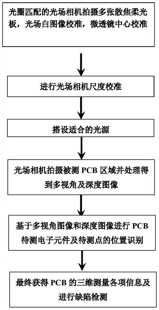
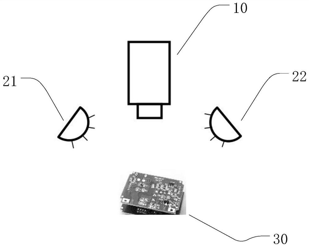
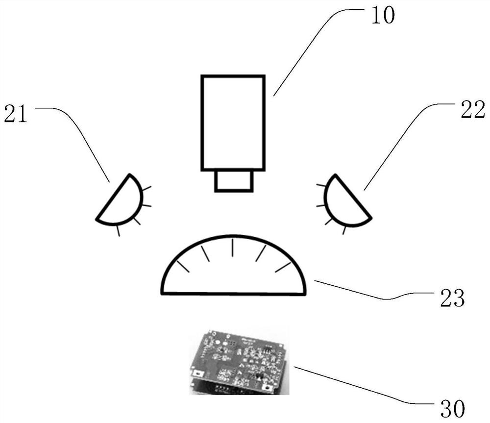
[0027] According to one or more embodiments, such as figure 2 As shown, a PCB inspection system includes a light field camera, the lens of the light field camera is facing the PCB to be inspected, and is used to obtain images including the soldering status of components on the PCB; two light sources, the light rays of these two light sources emit To the PCB to be tested, it is used to help the light field camera obtain an image of the soldering state of the PCB components.

[0028] According to one or more embodiments, such as figure 1 As shown, for the PCB inspection system, the inspection process for PCB includes,

[0029] Adjust the focal length and / or aperture of the light field camera to obtain a plurality of defocused soft light pure color calibration plates of the PCB components, and obtain a light field white image of the PCB components;

[0030] Calibrate the white image of the light field, and calibrate the center of the microlens of the light field camera;

[00...


PUM


Abstract

The invention provides a PCB detection system, which comprises a light field camera and at least one light source. The PCB detection process comprises the steps: adjusting the focal length and / or aperture of a light field camera, obtaining a plurality of defocused soft light pure color calibration boards of PCB components, and obtaining light field white images of the PCB components; calibrating the light field white images, and calibrating the center of the micro lens of the light field camera; performing scale calibration on the light field camera; erecting and adjusting the light source; shooting a detected PCB area through the light field camera to obtain a multi-view image and a depth image; according to the light field multi-view image and the depth image, carrying out position identification and positioning on the PCB component and a to-be-detected point; and finally, obtaining the three-dimensional size measurement information and defect detection information of the components of the detected PCB.

Description

technical field [0001] The invention belongs to the technical field of electronic processing and manufacturing, and in particular relates to a PCB and electronic component welding detection system and method. Background technique [0002] In recent years, with the rapid growth of science and technology and industrial level, the requirements for electronic products in daily life are getting higher and higher, and the demand is also increasing. Printed circuit board technology has improved the production speed of circuit boards to a certain extent, but with the high integration of PCB, the detection requirements and difficulty become more stringent, so PCB detection speed and accuracy have become a key factor restricting the production speed of this technology . The PCB (Printed Circuit Board, Chinese name is printed circuit board, hereinafter referred to as PCB) three-dimensional measurement and defect detection method belongs to the field of photoelectric detection technolo...

Claims


Application Information

Patent Timeline
IPC IPC(8): G01B11/00G01N21/95H05K13/08
CPCG01B11/002G01N21/9515H05K13/08
Inventor 丁俊飞李浩天
Owner VOMMA (SHANGHAI) TECH CO LTD
Why Eureka
Try Eureka