Cascaded sensing circuits for detecting and monitoring cracks in an integrated circuit

A technology for sensing circuits and integrated circuits, applied in the direction of circuits, measuring electricity, measuring electrical variables, etc.

Pending Publication Date: 2021-11-16
GLOBALFOUNDRIES U S INC MALTA
View PDF0 Cites 0 Cited by
  • Summary
  • Abstract
  • Description
  • Claims
  • Application Information

AI Technical Summary

Problems solved by technology

However, such crack detection structures are inherently flawed because they are designed to detect

Method used


Image

  • Cascaded sensing circuits for detecting and monitoring cracks in an integrated circuit
  • Cascaded sensing circuits for detecting and monitoring cracks in an integrated circuit
  • Cascaded sensing circuits for detecting and monitoring cracks in an integrated circuit

Examples


Example Embodiment

[0028] In the following description, reference is made to the accompanying drawings which form a part hereof, and in which is shown by way of illustration specific exemplary embodiments in which the present teachings may be practiced. These embodiments are described in sufficient detail to enable those skilled in the art to practice the teachings, and it is to be understood that other embodiments may be utilized and changes may be made without departing from the scope of the teachings. Accordingly, the following description is illustrative only.

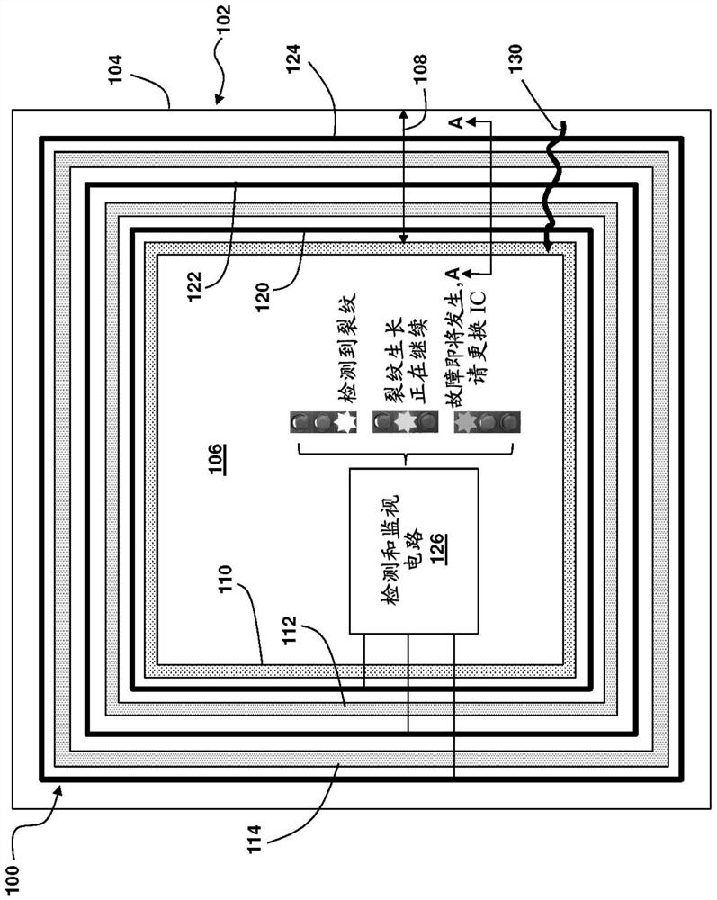
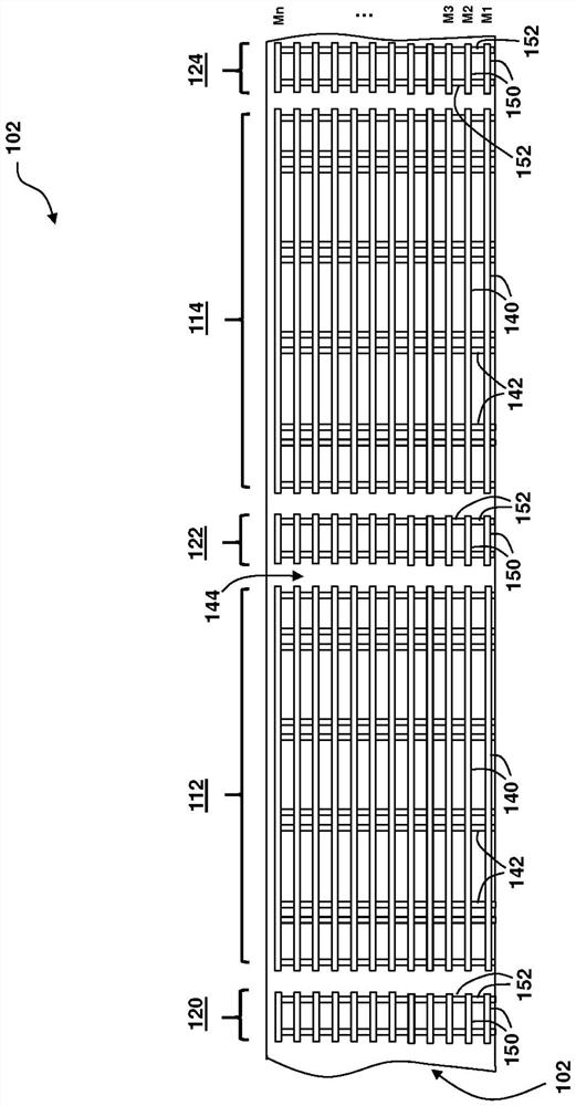
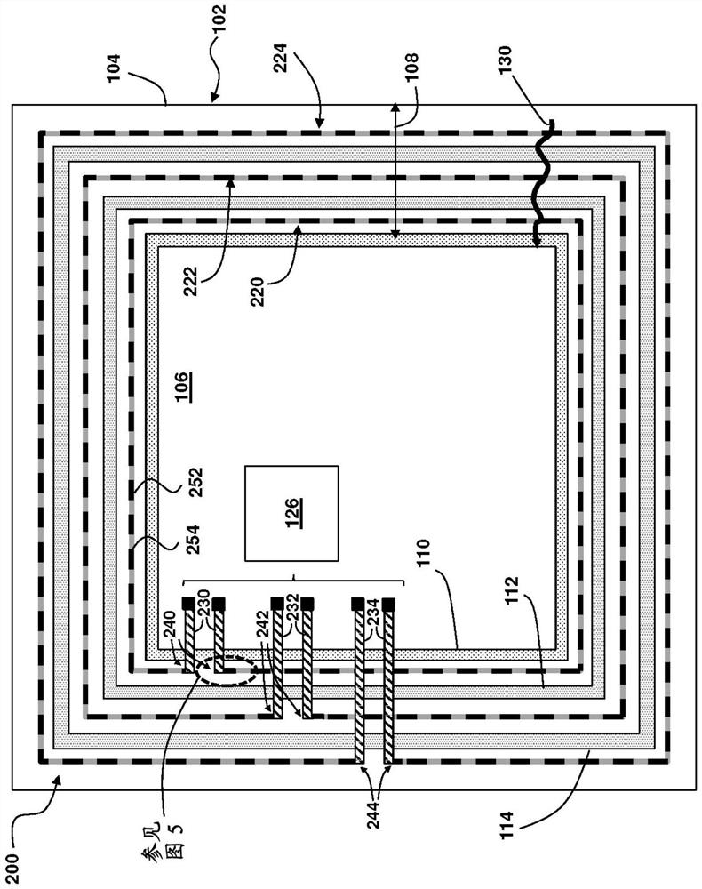
[0029] figure 1 Shown is a plan view of an integrated circuit (IC) 102 comprising a crack detection and monitoring system 100 for detecting and monitoring the growth of cracks according to an embodiment. The IC 102 is formed on a semiconductor substrate 104 (e.g., a silicon wafer) and includes an inner core (referred to below as the active region 106) surrounded by and passing through the guard ring 110 and at least one crack stop s...


PUM


Abstract

The invention relates to cascaded sensing circuits for detecting and monitoring cracks in an integrated circuit. Embodiments of the disclosure provide a crack detecting and monitoring system, including: a plurality of electrically conductive structures extending about a protective barrier formed in an inactive region of an integrated circuit (IC), wherein an active region of the IC is enclosed within the protective barrier; and a plurality of stages of sensing circuits connected in series for sensing a change in an electrical characteristic of each of the plurality of structures and for receiving an enable signal, wherein each sensing circuit is coupled to a respective structure of the plurality of structures, the change in the electrical characteristic indicating damage to the respective structure, and each sensing circuit includes a circuit for selectively generating the enable signal for a next sensing circuit in the plurality of stages of sensing circuits.

Description

technical field [0001] The present disclosure relates to integrated circuits, and more particularly to cascaded sensing circuits for detecting and monitoring cracks in integrated circuits (ICs). Background technique [0002] Processes such as wafer dicing can lead to the formation and propagation of cracks in ICs. Such cracks typically form at the interface between the dielectric material and the metal lines / contacts in the IC. [0003] ICs are often exposed to harsh, hostile and stressful environments (eg, automotive, aerospace, military, etc.). Fluctuations in environmental conditions (eg, changes in temperature, humidity, and air pressure) can exacerbate and activate slow crack growth mechanisms on both nascent and quiescent cracks (eg, cracks formed during wafer dicing) in ICs. Continuous fluctuations in environmental conditions can enhance the growth of nascent and quiescent cracks over time, potentially leading to IC failure. [0004] Crackstops (eg, interconnect st...

Claims


Application Information

Patent Timeline
IPC IPC(8): H01L23/544H01L21/66
CPCH01L22/34H01L22/12H01L22/20G01R31/2884G01R31/2853
Inventor 尼可拉斯·A·帕罗莫夫D·徐E·D·亨特-施罗德
Owner GLOBALFOUNDRIES U S INC MALTA
Why Eureka
Try Eureka