

Bias circuit
A technology of bias circuit and resistance, which is applied in the direction of electrical components, adjusting electrical variables, improving amplifiers to reduce temperature/power supply voltage changes, etc., and can solve problems such as bias voltage dependence and variation
- Summary
- Abstract
- Description
- Claims
- Application Information
AI Technical Summary
Problems solved by technology
Method used
Image

Examples
Embodiment approach
[0028] First, before describing the bias circuit according to the embodiment, the bias circuit according to the comparative example will be described.
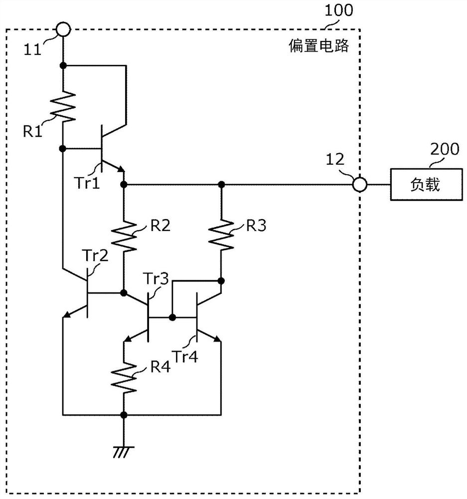
[0029] figure 1 It is a circuit configuration diagram showing an example of a bias circuit 100 according to a comparative example. In addition, the bias circuit according to the embodiment partially has the same circuit configuration as the bias circuit 100 according to the comparative example, and detailed description of each component included in the bias circuit 100 will be omitted here.
[0030] In the bias circuit 100 according to the comparative example, instead of a current source using a P-channel transistor or a depletion FET, the resistor R1 is used to reduce the cost of the bias circuit 100 . A current corresponding to the power supply voltage supplied from the terminal 11 can flow through the resistor R1, so the resistor R1 can be used instead of the current source. However, for example, when the power supply vol...
Deformed example 1
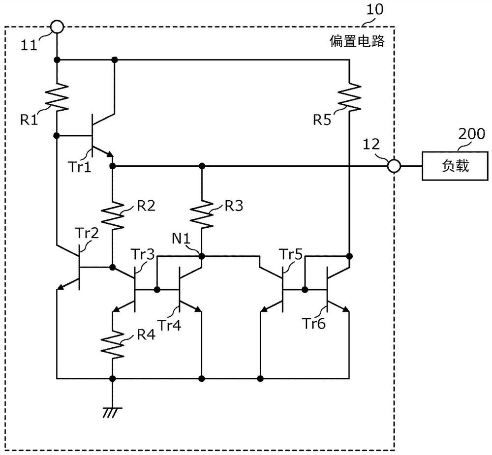
[0074] Next, a bias circuit according to Modification 1 will be described.
[0075] Figure 5 It is a circuit configuration diagram showing an example of a bias circuit 10a according to Modification 1.
[0076] The bias circuit 10a according to Modification 1 is different from the bias circuit 10 according to the embodiment in that the transistor Tr1 is an FET (specifically, an enhancement type FET). Other points are the same as those of the bias circuit 10 according to the embodiment, and therefore description thereof will be omitted.
[0077] Since the transistor Tr1 is an FET, the bias circuit 10a can supply a stable bias voltage compared to the case where the transistor Tr1 is a bipolar transistor. This is because the voltage drop between the gate and source of a FET is less dependent on temperature than a bipolar transistor. In addition, since the amount of voltage drop between the gate and the source of the transistor Tr1 is smaller than that of a bipolar transistor, ...
Deformed example 2
[0079] Next, a bias circuit according to Modification 2 will be described.
[0080] Image 6 It is a circuit configuration diagram showing an example of a bias circuit 10b according to Modification 2.
[0081] The bias circuit 10b according to Modification 2 differs from the bias circuit 10a according to Modification 1 in that it further includes a resistor R6, and the first terminal of the transistor Tr1, the fifth terminal of the transistor Tr2, and the other end of the resistor R1 are connected to each other. , and connected to terminal 12 (specifically, the first terminal of transistor Tr1 and the other end of resistor R1 are connected to terminal 12 via resistor R6), the third terminal of transistor Tr1, one end of resistor R2 and one end of resistor R3 are connected to each other. Other points are the same as those in the bias circuit 10 a according to Modification 1, and thus description thereof will be omitted. In addition, the load current flowing through the load 2...
PUM
 Abstract
Description
Claims
Application Information