A circuit structure for lcd driving bias voltage

A bias voltage and circuit structure technology, applied in electronic switches, electrical components, pulse technology, etc., can solve the problems of increased cost and no advantages of aluminum gate technology, and achieve small chip area occupation, low cost, and stable bias voltage Effect

Active Publication Date: 2022-07-26
SHENZHEN HANGSHUN CHIP TECH DEV CO LTD
View PDF0 Cites 0 Cited by
  • Summary
  • Abstract
  • Description
  • Claims
  • Application Information

AI Technical Summary

Problems solved by technology

[0002] The bias voltage circuit used for LCD driving in traditional integrated circuits usually adopts aluminum gate technology, and the plate capacitor composed of aluminum layer and N+ or P+ does not need to add additional masks. With the improvement of integrated circuit integration, The aluminum gate process has no advantage in cost. In the silicon gate process, an additional photomask is required to make a plate capacitor (a plate capacitor composed of polycrystalline and N+ or P+), which increases the cost.

Method used


Image

  • A circuit structure for lcd driving bias voltage

Examples


Embodiment Construction

[0014] The present invention will be further described below in conjunction with the accompanying drawings and embodiments:

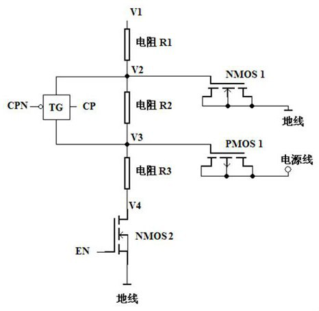
[0015] like figure 1 As shown, a circuit structure for LCD driving bias voltage includes a resistor R1, a resistor R2, a resistor R3, a first NMOS transistor, a second NMOS transistor, a PMOS transistor and a transmission gate TG, the resistor R1, the The size of the resistor R2 and the resistor R3 are the same or not much different. The output end of the resistance R1 is respectively connected with one end of the transmission gate TG, the input end of the resistance R2 and the input end of the first NMOS transistor, one end of the transmission gate TG, the input end of the resistance R2 The terminal and the input terminal of the first NMOS transistor are connected to each other, and the output terminal of the resistor R2 is respectively connected to the other terminal of the transmission gate TG, the input terminal of the resistor R3 and the input ter...


PUM


Abstract

The invention discloses a circuit structure for LCD driving bias voltage, comprising resistor R1, resistor R2, resistor R3, a first NMOS transistor, a second NMOS transistor, a PMOS transistor and a transmission gate TG. The output ends of the resistor R1 are respectively It is connected to one end of the transmission gate TG, the input end of the resistor R2 and the input end of the first NMOS tube, and the output end of the resistor R2 is respectively connected to the other end of the transmission gate TG, the input end of the resistor R3 and the input end of the PMOS tube. The output end of R3 is connected to the input end of the second NMOS transistor. By adopting NMOS tube and PMOS tube, the present invention has stable bias voltage, good effect, simple structure, high circuit integration, small occupied chip area and low cost.

Description

technical field [0001] The invention relates to the technical field of integrated circuit structures, in particular to a circuit structure for LCD driving bias voltage. Background technique [0002] The bias voltage circuit used for LCD driving in traditional integrated circuits usually adopts aluminum gate technology, and the plate capacitor composed of aluminum layer and N+ or P+ does not need to add additional masks. With the improvement of integrated circuit integration, The aluminum gate process has no advantage in cost. In the silicon gate process, an additional mask is required to fabricate a plate capacitor (a plate capacitor composed of polycrystalline and N+ or P+), thereby increasing the cost. The above shortcomings are worth solving. SUMMARY OF THE INVENTION [0003] In order to overcome the deficiencies of the prior art, the present invention provides a circuit structure for LCD driving bias voltage. [0004] The technical scheme of the present invention is ...

Claims


Application Information

Patent Timeline
Patent Type & Authority Patents(China)
IPC IPC(8): G09G3/36H03K17/687
CPCG09G3/3696H03K17/687
Inventor 刘吉平张怀东周蕴言冯冰
Owner SHENZHEN HANGSHUN CHIP TECH DEV CO LTD
Why Eureka
Try Eureka