Formation method of semiconductor structure

A semiconductor and gate structure technology, applied in the field of semiconductor structure formation, can solve the problems of easy short circuit of interconnect structure, open circuit between interconnect structure and device, affecting the performance and reliability of semiconductor device, etc., so as to improve performance and reliability, improve Graphics Accuracy, Performance-Boosting Effects

Pending Publication Date: 2021-12-17
SEMICON MFG INT (SHANGHAI) CORP +1
View PDF0 Cites 0 Cited by
  • Summary
  • Abstract
  • Description
  • Claims
  • Application Information

AI Technical Summary

Problems solved by technology

[0003] However, with the increase of device density, it is easy to short circuit between the formed interconnection structures; the continuous reduction of the critical dimension of the interconnection structure will also easily lead to an open circuit between the interconnection structure and the device, thereby affecting the performance and reliability of semiconductor devices. sex

Method used


Image

  • Formation method of semiconductor structure
  • Formation method of semiconductor structure
  • Formation method of semiconductor structure

Examples


Embodiment Construction

[0033] As mentioned in the background art, the performance and reliability of semiconductor devices are affected because the formed interconnection structures are easily short-circuited, or the formed interconnection structures and devices are easily disconnected. Now analyze and illustrate in conjunction with specific embodiment.

[0034] It should be noted that the "surface" in this specification is used to describe the relative positional relationship in space, and is not limited to direct contact.

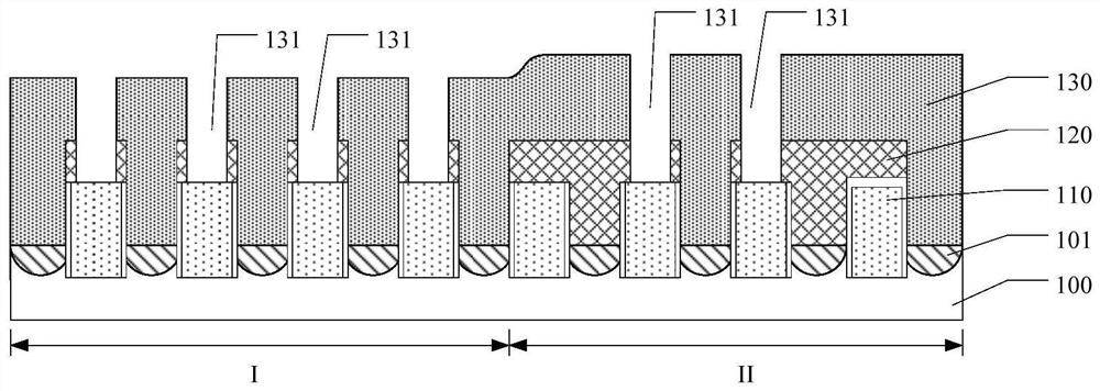
[0035] Figure 1 to Figure 2 It is a structural schematic diagram of each step in the formation process of a semiconductor structure.

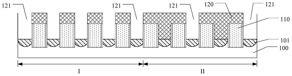
[0036] Please refer to figure 1 , providing a substrate, the substrate includes a first region I and a second region II, the substrate further includes a base 100 and several fins (not shown) separated from each other on the surface of the base 100, and, There are several source-drain doped layers 101 between adjacent fins; several gate stru...


PUM

PropertyMeasurementUnit
Thicknessaaaaaaaaaa

Abstract

A method for forming a semiconductor structure comprises the following steps: providing a substrate which comprises a first region and a second region; forming a plurality of source-drain doping layers, a plurality of gate structures and an initial first dielectric layer in the substrate in the first region and the second region respectively; forming a first mask layer on the surface of the initial first dielectric layer, wherein a plurality of first openings are formed in the first mask layer on the first region and the first mask layer on the second region respectively, the first openings are located in the source-drain doping layer, and the density of the first openings in the first region is different from the density of the first openings in the second region; and forming a plurality of second openings in the first mask layer of the first region and the second region, wherein the second openings are located on the gate structure. Therefore, the performance and the reliability of the semiconductor structure are improved.

Description

technical field [0001] The invention relates to the technical field of semiconductor manufacturing, in particular to a method for forming a semiconductor structure. Background technique [0002] With the development of semiconductor technology, the chip integration level of ultra-large-scale integrated circuits (ULSI) has reached hundreds of millions or even billions of devices, and multi-level metal interconnection technology (Multi-level Metal Interconnect) is widely used. [0003] However, with the increase of device density, it is easy to short circuit between the formed interconnection structures; the continuous reduction of the critical dimension of the interconnection structure will also easily lead to an open circuit between the interconnection structure and the device, thereby affecting the performance and reliability of semiconductor devices. sex. Contents of the invention [0004] The technical problem solved by the invention is to provide a method for forming ...

Claims


Application Information

Patent Timeline
IPC IPC(8): H01L21/768
CPCH01L21/76847H01L21/76879H01L21/7688H01L21/76831
Inventor 刘洋
Owner SEMICON MFG INT (SHANGHAI) CORP
Why Eureka
Try Eureka