Double-sided display panel and manufacturing method thereof

A double-sided display and panel technology, which is applied in nonlinear optics, instruments, optics, etc., can solve problems such as inability to meet double-sided display

Inactive Publication Date: 2022-01-04
HKC CORP LTD
View PDF5 Cites 1 Cited by
  • Summary
  • Abstract
  • Description
  • Claims
  • Application Information

AI Technical Summary

Problems solved by technology

The reflective display is to install reflective material under the liquid crystal display panel to replace the luminescent material of the transmissive display. When the ambient light is sufficient, it uses the light reflected by the mirror to illuminate the screen to achieve the effect of displaying the picture. ; while the existing reflective display screens on the market are all single-sided display, which cannot meet the needs of double-sided display in some special cases

Method used


Image

  • Double-sided display panel and manufacturing method thereof
  • Double-sided display panel and manufacturing method thereof
  • Double-sided display panel and manufacturing method thereof

Examples


no. 1 example

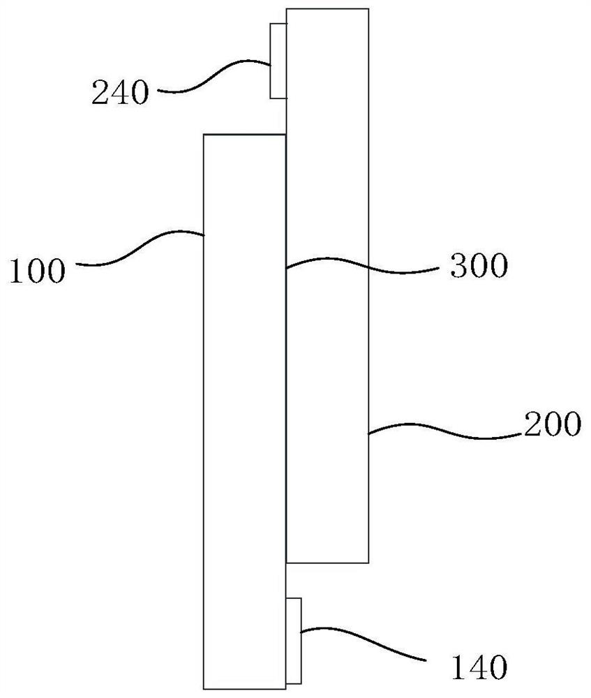
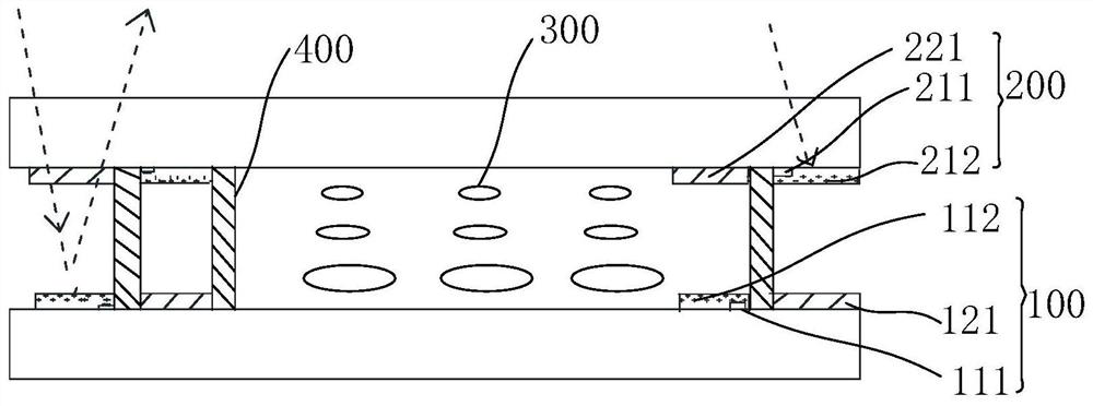
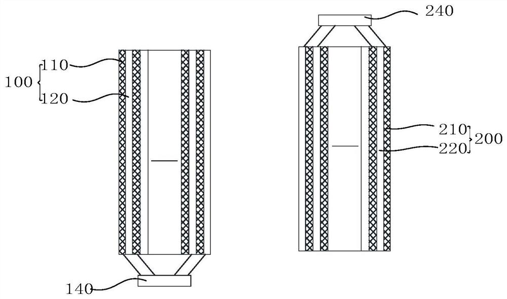
[0038] figure 1 is a schematic diagram of a double-sided display panel provided in the first embodiment of the present application, as shown in figure 1 As shown, a double-sided display panel 10 includes a first substrate 100, a second substrate 200 and a liquid crystal layer 300, the first substrate 100 and the second substrate 200 are oppositely arranged, and the first substrate 100 and the A liquid crystal layer 300 is arranged between the second substrates 200, the first substrate 100 includes a first reflective region 110 and a first transparent region 120, and the first reflective region 110 and the first transparent region 120 are arranged on the first The side of the substrate 100 close to the second substrate 200, the second substrate 200 includes a second reflective region 210 and a first transparent region 120, the second reflective region 210 and the second transparent region 220 are arranged on the first The second substrate 200 is close to the side of the first ...

no. 2 example

[0053] Figure 5 is a schematic diagram of a first substrate and a second substrate provided in the second embodiment of the present application, as shown in Figure 5 As shown, the difference between this embodiment and the first embodiment is that the first reflective regions 110 are arranged in rows along the data line direction to obtain the first reflective region rows, and the first transparent regions 120 are arranged in rows along the data line direction. arranging to obtain the first transparent region row, the first reflective region row and the first transparent region row are arranged at intervals; the second reflective region 210 is arranged in row along the data line direction to obtain the second reflective region row, The second transparent regions 220 are arranged in rows along the data line direction to obtain rows of second transparent regions, the rows of second reflective regions and the rows of second transparent regions are arranged at intervals between ...

no. 3 example

[0056] Figure 6 It is a schematic diagram of a first substrate and a second substrate provided in the third embodiment of the present application, as shown in Figure 6 As shown, the difference between this embodiment and the first and second embodiments is that the first reflective region 110 and the first transparent region 120 are arranged at regular intervals along the direction of the data line and the direction of the scan line; The two reflective regions 210 and the second transparent regions 220 are evenly arranged at intervals along the direction of the data line and the direction of the scan line. That is, in the horizontal direction, the first reflective regions 110 and the first transparent regions 120 in the first row are arranged evenly and evenly, and at the same time, the second reflective regions 210 and the second transparent regions 220 are arranged evenly and oddly; The regions 110 and the first transparent regions 120 are evenly arranged, while the secon...


PUM


Abstract

The invention discloses a double-sided display panel and a manufacturing method thereof. The double-sided display panel comprises a first substrate, a second substrate and a liquid crystal layer; the first substrate and the second substrate are oppositely arranged; the liquid crystal layer is arranged between the first substrate and the second substrate; the first substrate comprises a first reflection area and a first transparent area; the second substrate comprises a second reflection area and a second transparent area; the first reflection area and the first transparent area are arranged on the side, close to the second substrate, of the first substrate; the second substrate comprises a second reflection area and a first transparent area; and the second reflection area and the second transparent area are arranged on the side, close to the first substrate, of the second substrate; the first reflection area corresponds to the second transparent area; and the first transparent area corresponds to the second reflection area. By means of the above design, due to the fact that the reflection area of the first substrate corresponds to the transparent area of the second substrate, and the reflection area of the second substrate corresponds to the transparent area of the first substrate, double-sided display is achieved.

Description

technical field [0001] The present application relates to the field of display technology, in particular to a double-sided display panel and a manufacturing method thereof. Background technique [0002] Liquid Crystal Display (LCD) has many advantages such as thin body, power saving, and no radiation, and has been widely used, such as: mobile phones, personal digital assistants (PDA), digital cameras, computer screens and notebook computers screen etc. [0003] In the prior art, a liquid crystal display panel in a liquid crystal display device includes a color filter substrate (ColorFilter Substrate) and a thin film transistor array substrate (Thin Film Transistor Array Substrate, TFT Array Substrate) disposed opposite to each other, and a color filter substrate and a TFT array substrate disposed between the color filter substrate and the TFT array substrate. The working principle of the liquid crystal layer (Liquid Crystal Layer) in between is to control the rotation of th...

Claims


Application Information

Patent Timeline
Patent Type & Authority Applications(China)
IPC IPC(8): G02F1/1333
CPCG02F1/133342
Inventor 夏天宇郑浩旋
Owner HKC CORP LTD
Why Eureka
Try Eureka