A display substrate and a display device

A technology for display substrates and backplanes, which is used in the identification of devices, instruments, semiconductor devices, etc., can solve the problems of large-scale transfer of Micro-LED displays, complex display circuit layout, etc., and reduce the workload of massive transfer. volume, added functionality and interesting effects

Active Publication Date: 2021-06-22
CHONGQING KONKA PHOTOELECTRIC TECH RES INST CO LTD
View PDF4 Cites 0 Cited by
  • Summary
  • Abstract
  • Description
  • Claims
  • Application Information

AI Technical Summary

Problems solved by technology

[0005] In view of the deficiencies in the prior art above, the purpose of the present invention is to provide a display substrate and a display device, which overcomes the fact that the existing Micro-LED displays can only realize single-sided display and need to install 3 LEDs on the backplane. Chips are composed of pixel units, which makes the workload of Micro-LED display huge transfer very huge, and the defect of complex circuit arrangement of the display

Method used


Image

  • A display substrate and a display device
  • A display substrate and a display device
  • A display substrate and a display device

Examples


Embodiment Construction

[0047] In order to make the object, technical solution and advantages of the present invention more clear and definite, the present invention will be further described in detail below with reference to the accompanying drawings and examples. It should be understood that the specific embodiments described here are only used to explain the present invention, not to limit the present invention.

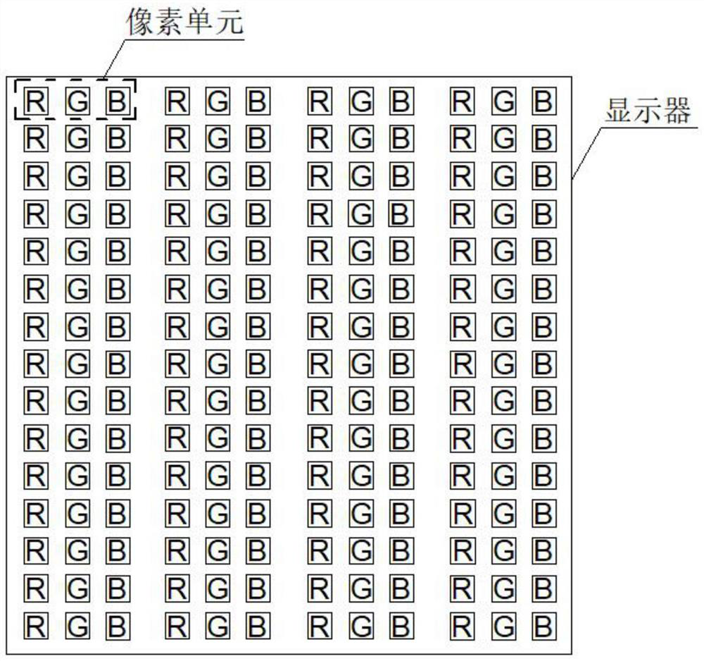
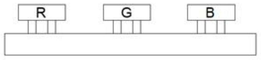
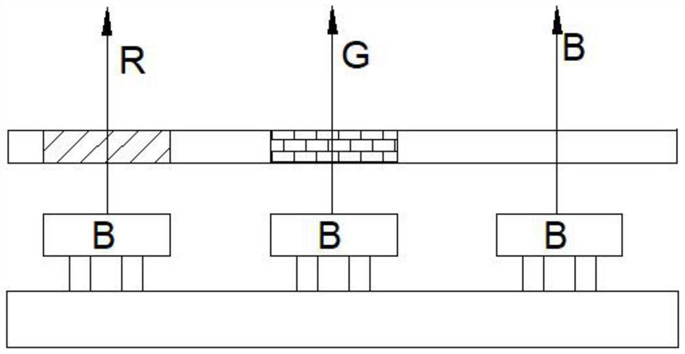
[0048] Since the existing Micro-LED displays can only realize single-sided display, and need to install 3 LED chips on the backplane to form a pixel unit, the workload of mass transfer of Micro-LED displays is very huge, and the circuit layout of the display is complicated. defect. In order to solve the above problems, Embodiment 1 of the present invention provides a display substrate, such as Figure 4 As shown, the display substrate includes a backplane 1 and a plurality of pixel units 2 . The pixel unit 2 includes a white light LED 21 arranged on the back plate 1 for emitting a whit...


PUM

PropertyMeasurementUnit
wavelengthaaaaaaaaaa

Abstract

The present invention provides a display substrate and a display device. The display substrate includes: a backplane and a plurality of pixel units; the pixel units include white LEDs; a collimating lens for collimating white light beams; A prism layer for reflecting monochromatic light of different colors in the first direction and a second direction; a transmittance controller for modulating the transmittance of monochromatic light of different colors; A scattering layer that scatters monochromatic light. In this application, the white light beam is reflected by the prism layer to obtain monochromatic light of different colors in the first direction and the second direction, and the monochromatic light of different colors is modulated by the transmittance controller to generate the corresponding pixel unit Color, realizes the double-sided display of the Micro-LED display, increases the functionality and interest of the display, and reduces the huge transfer workload of the Micro-LED display and the complexity of the display circuit layout.

Description

technical field [0001] The invention belongs to the technical field of semiconductor optoelectronics, and in particular relates to a display substrate and a display device. Background technique [0002] Micro-LED display has good stability, lifespan, and advantages in operating temperature, and also inherits the advantages of LED low power consumption, color saturation, fast response, strong contrast, etc. Micro-LED has higher brightness, and The lower power consumption makes Micro-LED displays have great application prospects. [0003] The structure diagram of the display substrate of the current Micro-LED display is as follows: figure 1 and figure 2 As shown, the display substrate of the existing Micro-LED display is composed of a backplane and a plurality of pixel units arranged on the backplane, and each pixel unit includes red LEDs, green LEDs and blue LEDs arranged in sequence. In order to save costs, there are also existing image 3 The display substrate of the M...

Claims


Application Information

Patent Timeline
Patent Type & Authority Patents(China)
IPC IPC(8): H01L33/58G09F9/33
CPCH01L33/58G09F9/33H01L2933/0091H01L25/0753H01L25/167H01L33/60G02B5/045G02B27/102G02B27/141G02B27/145G02B5/0278G02B5/26G02B27/30
Inventor 袁山富向毅
Owner CHONGQING KONKA PHOTOELECTRIC TECH RES INST CO LTD
Why Eureka
Try Eureka