Supercharge Your Innovation With Domain-Expert AI Agents!

Optoelectronic device testing device

A technology for optoelectronic devices and testing devices, which is applied in the testing of optical instruments, measuring devices, and testing of machinery/structural components, etc., can solve the problem of low testing efficiency and achieve good testing results, increase stability, and improve efficiency.

Pending Publication Date: 2022-01-07
新沂崚峻光电科技有限公司
View PDF0 Cites 0 Cited by
  • Summary
  • Abstract
  • Description
  • Claims
  • Application Information

AI Technical Summary

Problems solved by technology

[0003] However, most of the existing optoelectronic device testing devices are mostly tested individually. Such testing efficiency is not high and has certain limitations. Therefore, we propose a optoelectronic device testing device to solve the above technical problems

Method used


Image

  • Optoelectronic device testing device
  • Optoelectronic device testing device
  • Optoelectronic device testing device

Examples


Embodiment Construction

[0024] The following will clearly and completely describe the technical solutions in the embodiments of the present invention with reference to the accompanying drawings in the embodiments of the present invention. Obviously, the described embodiments are only some, not all, embodiments of the present invention. Based on the embodiments of the present invention, all other embodiments obtained by persons of ordinary skill in the art without making creative efforts belong to the protection scope of the present invention.

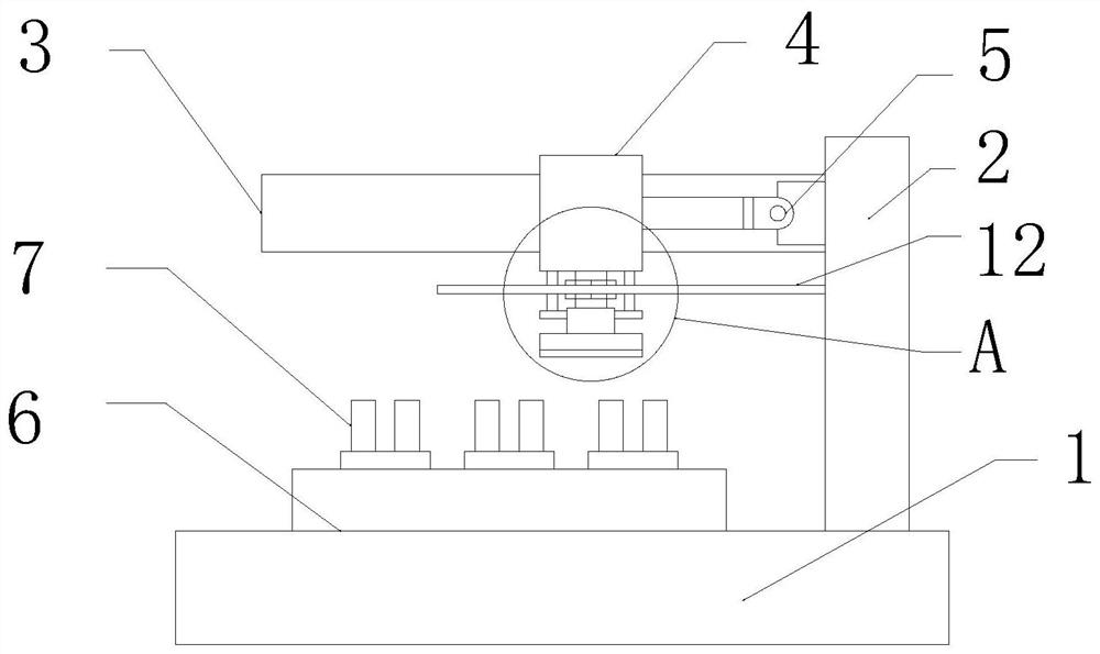
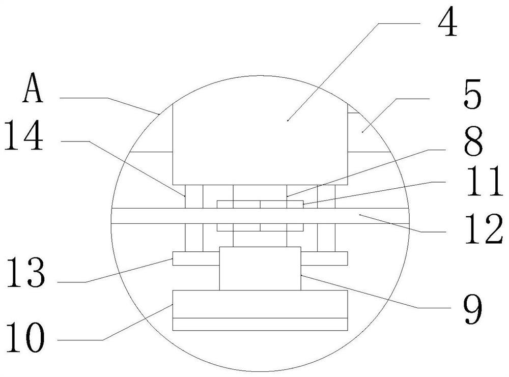
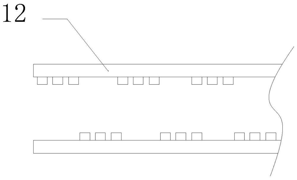
[0025] see Figure 1-3 , an optoelectronic device testing device, comprising a base 1, a support column 2 is fixedly installed on the top of one side of the base 1, a movable column 3 is fixedly installed on one side of the top of the support column 2, and a movable sleeve is movably installed on the outer surface of the movable column 3 4. A cylinder 5 is arranged between the movable sleeve 4 and the support column 2, and the cylinder 5 is used to drive the m...


PUM


Abstract

The invention relates to the technical field of optoelectronic device testing, and discloses an optoelectronic device testing device which comprises a base, a supporting column is fixedly installed at the top end of one side of the base, a movable column is fixedly installed on one side of the top end of the supporting column, and a movable sleeve is movably installed on the outer surface of the movable column. An air cylinder is arranged between the movable sleeve and the supporting column, a machining plate is fixedly installed at the top end of the base, a placement base is arranged at the top end of the machining plate, a threaded column is movably installed at the bottom end of the movable sleeve, and the other end of the threaded column is in threaded connection with a threaded sleeve. According to the invention, through the arrangement of the placement base, the threaded column, the threaded sleeve, the driving gear, the dislocation rack, the movable sleeve, the air cylinder and other structures, the optoelectronic device placed at the placement base can be tested in a reciprocating mode, so that the testing efficiency is improved, the testing device has the advantages of being good in testing effect and the like, and the technical problems are solved.

Description

technical field [0001] The invention relates to the technical field of optoelectronic device testing, in particular to an optoelectronic device testing device. Background technique [0002] Optoelectronic devices are various functional devices made using the electro-photon conversion effect. The design principle of optoelectronic devices is based on the change of the propagation mode of guided wave light by the external field. It is also different from the optoelectronic devices used by early people. When testing optoelectronic devices An optoelectronic device test setup is required. [0003] However, most of the existing optoelectronic device testing devices are mostly tested individually. Such testing efficiency is not high and has certain limitations. Therefore, we propose an optoelectronic device testing device to solve the above technical problems. Contents of the invention [0004] (1) Solved technical problems [0005] Aiming at the deficiencies of the prior art, ...

Claims


Application Information

Patent Timeline
Patent Type & Authority Applications(China)
IPC IPC(8): G01R31/01G01R1/04G01M11/00
CPCG01R31/013G01R1/0408G01M11/00
Inventor 吴迪
Owner 新沂崚峻光电科技有限公司
Features
  • R&D
  • Intellectual Property
  • Life Sciences
  • Materials
  • Tech Scout
  • Unparalleled Data Quality
  • Higher Quality Content
  • 60% Fewer Hallucinations
Learn More