Supercharge Your Innovation With Domain-Expert AI Agents!

Semiconductor process equipment and impedance matching method thereof

A technology of impedance matching and process equipment, applied in semiconductor/solid-state device manufacturing, impedance network, discharge tube, etc., can solve the problem of low impedance matching efficiency, and achieve the effect of improving impedance matching efficiency and shortening impedance matching time.

Pending Publication Date: 2022-01-11
BEIJING NAURA MICROELECTRONICS EQUIP CO LTD
View PDF0 Cites 1 Cited by
  • Summary
  • Abstract
  • Description
  • Claims
  • Application Information

AI Technical Summary

Problems solved by technology

[0005] The purpose of the embodiment of the present application is to provide a semiconductor process equipment and its impedance matching method to solve the problem of low impedance matching efficiency in the existing semiconductor process

Method used


Image

  • Semiconductor process equipment and impedance matching method thereof
  • Semiconductor process equipment and impedance matching method thereof
  • Semiconductor process equipment and impedance matching method thereof

Examples


Embodiment Construction

[0022] The present application embodiment provides a semiconductor process device and its impedance matching method to solve the problem of lower impedance matching efficiency during existing semiconductor processes.

[0023] In order to better understand the technical solutions in the present application, the technical solutions in the present application embodiment will be described in connection with the drawings in the present application, and EXAMPLES Embodiments are merely embodiments of the present invention, not all of the embodiments. Based on the embodiments in the present application, those of ordinary skill in the art should belong to the scope of the present application without all other embodiments obtained by creative labor.

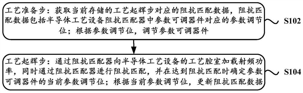
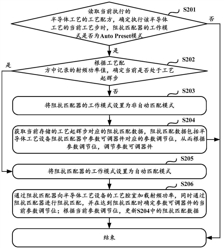
[0024] figure 1 It is a schematic flow diagram of an impedance matching method applied to a semiconductor process apparatus according to an embodiment of the present application. like figure 1 Distance figure 1 The method can include:

[0025...


PUM


Abstract

The embodiment of the invention discloses semiconductor process equipment and an impedance matching method thereof, which are used for solving the problem of low impedance matching efficiency in the existing semiconductor process. The method comprises the following steps of in a process preparation step, acquiring currently stored impedance matching data corresponding to a process build-up step, wherein the impedance matching data comprises a parameter adjusting position corresponding to a parameter adjustable device in an impedance matcher of semiconductor process equipment, and adjusting the parameter adjustable device according to the parameter adjusting position, in a process build-up step, loading radio frequency power to a process chamber of the semiconductor process equipment through an impedance matcher, performing impedance matching through the impedance matcher, and determining a current parameter adjusting position of the parameter adjustable device when the impedance matching is achieved, and updating the impedance matching data according to the current parameter adjusting position. According to the technical scheme, the parameter adjustable device can be accurately and automatically adjusted according to the parameter adjusting position in the impedance matching data, the impedance matching time is shortened, and the impedance matching efficiency is improved.

Description

Technical field [0001] The present application relates to the field of semiconductor technology, and more particularly to a semiconductor process device and its impedance matching method. Background technique [0002] Inductive coupling plasma sources are applied to etching, film deposition, ion implantation, etc. in the semiconductor equipment manufacturing. The plasma reaction chamber has inductive coupling coils and electrostatic chucks, in the etching field, the main principle of the inductive coupling plasma source is: the radio frequency current flows through the inductive coupling coil, thereby generating an electromagnetic field in the reaction chamber, an electromagnetic field exciting the reaction chamber. The access gas generates a plasma, and the bias source control ion bombardment energy allows the plasma to accelerate the silicon sheet to achieve etching. Among them, the silicon wafer is attached to the electrostatic chuck by electrostatic adsorption. [0003] In a ...

Claims


Application Information

Patent Timeline
Patent Type & Authority Applications(China)
IPC IPC(8): H01J37/32H01L21/67H03H7/40
CPCH01J37/32183H01J37/32137H03H7/40H01L21/67069H03H7/38H01J37/32082H01J37/32174H01J2237/327H01L22/20
Inventor 李文庆韦刚杨京蒋书棋张迪
Owner BEIJING NAURA MICROELECTRONICS EQUIP CO LTD
Features
  • R&D
  • Intellectual Property
  • Life Sciences
  • Materials
  • Tech Scout
  • Unparalleled Data Quality
  • Higher Quality Content
  • 60% Fewer Hallucinations
Learn More