Array substrate, display panel and display device

A technology for array substrates and substrate substrates, applied in static indicators, semiconductor/solid-state device parts, instruments, etc., can solve problems such as unstable gate voltage of drive transistors, improve display effects, improve luminous accuracy, Effect of simplified pixel circuit structure

Pending Publication Date: 2022-01-14
WUHAN TIANMA MICRO ELECTRONICS CO LTD
View PDF13 Cites 7 Cited by
  • Summary
  • Abstract
  • Description
  • Claims
  • Application Information

AI Technical Summary

Problems solved by technology

[0004] The present invention provides an array substrate, a display panel and a display device to improve the problem of unstable gate voltage of the drive transistor caused by the leakage current of the lead transistor and improve the display effect

Method used


Image

  • Array substrate, display panel and display device
  • Array substrate, display panel and display device
  • Array substrate, display panel and display device

Examples


Embodiment Construction

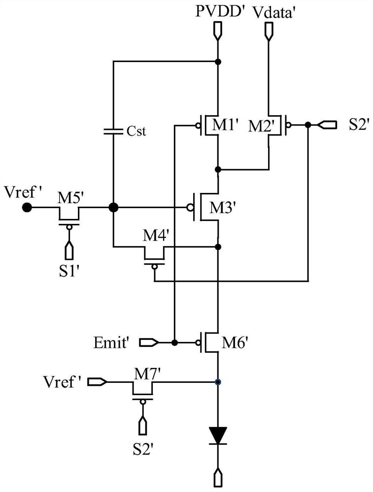
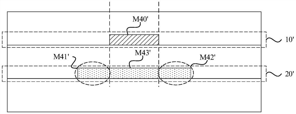
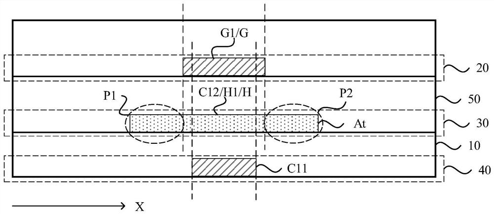
[0033] The present invention will be further described in detail below in conjunction with the accompanying drawings and embodiments. It should be understood that the specific embodiments described here are only used to explain the present invention, but not to limit the present invention. In addition, it should be noted that, for the convenience of description, only some structures related to the present invention are shown in the drawings but not all structures. It will be apparent to those skilled in the art that various modifications and variations can be made in the present invention without departing from the spirit or scope of the inventions. Therefore, the present invention is intended to cover the modifications and variations of the present invention falling within the scope of the corresponding claims (technical solutions to be protected) and their equivalents. It should be noted that, the implementation manners provided in the embodiment of the present invention ma...


PUM


Abstract

The invention discloses an array substrate. The array substrate comprises a pixel circuit which comprises a driving transistor, at least one first switching transistor, and at least one compensation capacitor. A part of the channel of the first switching transistor is multiplexed as a polar plate of the compensation capacitor. According to the embodiment of the invention, the variable quantity of the grid voltage of the first switching transistor is divided through the compensation capacitor, so that the voltage coupled to the channel of the first switching transistor due to the jump of the grid voltage of the first switching transistor can be reduced, and the leakage current generated by the first switching transistor is reduced; therefore, the situation that the grid potential of the driving transistor is unstable due to the leakage current is improved, the light emitting stability of a light emitting element driven by the pixel circuit is improved, especially the phenomena of flickering and screen shaking under low-frequency driving can be improved, and the display effect is improved.

Description

technical field [0001] Embodiments of the present invention relate to the field of display technology, and in particular, to an array substrate, a display panel, and a display device. Background technique [0002] Organic Light-Emitting Diode (OLED) display panels have broad application prospects due to their advantages such as self-illumination, high contrast ratio, thin thickness, fast response speed, and being applicable to flexible panels. [0003] The OLED element of the OLED display panel is a current-driven element, and a corresponding pixel driving circuit needs to be provided to provide a driving current for the OLED element so that the OLED element can emit light. The pixel driving circuit of an OLED display panel generally includes a driving transistor and at least one switching transistor, etc., and the switching transistor can write a corresponding signal to the gate of the driving transistor, so that in the light-emitting phase, the driving transistor can gener...

Claims


Application Information

Patent Timeline
Patent Type & Authority Applications(China)
IPC IPC(8): H01L29/10H01L23/64H01L27/32G09G3/3233G09G3/3266
CPCH01L29/1033H01L28/60G09G3/3233G09G3/3266G09G2320/0247H10K59/121H10K59/1216
Inventor 匡建张蒙蒙吴员涛
Owner WUHAN TIANMA MICRO ELECTRONICS CO LTD
Why Eureka
Try Eureka