An electronic seal stamping method, system, electronic device and readable medium

An electronic stamp and stamp technology, applied in image analysis, image enhancement, graphics and image conversion, etc., can solve the problems of lack of resolution, low efficiency of electronic stamps, limited operation scenarios, etc., to ensure size consistency, reduce application conditions and The effect of operational difficulty

Active Publication Date: 2022-07-22
广州市新文溯科技有限公司
View PDF4 Cites 0 Cited by
  • Summary
  • Abstract
  • Description
  • Claims
  • Application Information

AI Technical Summary

Problems solved by technology

This has restrictions on the scanning equipment for obtaining electronic seals, the operating requirements for scanning operations, and the way to obtain target documents
These harsh conditions lead to inefficiency in the operation of electronic seals, and greatly limit the operation scenarios
[0004] Moreover, in the process of creating an electronic stamp, due to the inconsistency between the resolution of the scanning device and the resolution of the stamped target document, or the lack of resolution caused by sending the image document under abnormal operation, this will make the After stamping the target document with an electronic stamp, the printed stamp may be seriously inconsistent with the actual stamp size, and the printed stamp and the actual stamp size will be significantly enlarged or reduced

Method used


Image

  • An electronic seal stamping method, system, electronic device and readable medium
  • An electronic seal stamping method, system, electronic device and readable medium
  • An electronic seal stamping method, system, electronic device and readable medium

Examples


Embodiment Construction

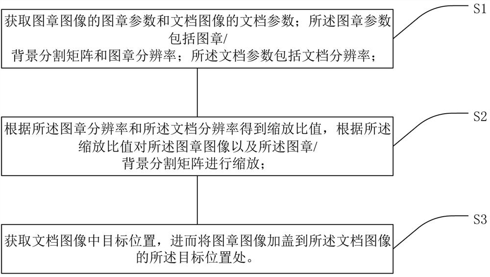
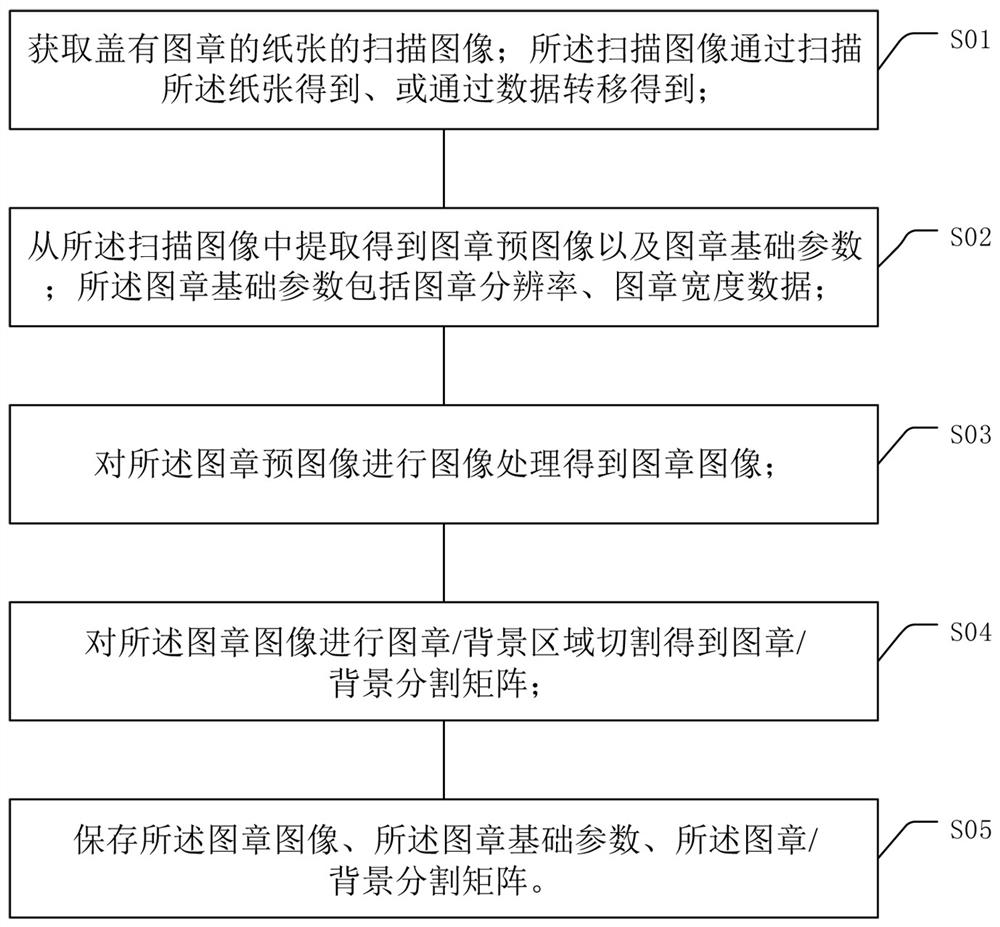
[0048] In order to make the objectives, technical solutions and effects of the present invention clearer and clearer, the present invention will be further described in detail below with reference to the accompanying drawings and examples. It should be understood that the specific embodiments described herein are only used to explain the present invention, but not to limit the present invention.

[0049] It should be understood by those skilled in the art that the foregoing general description and the following detailed description are exemplary and illustrative of specific embodiments of the present invention and are not intended to limit the present invention.

[0050] The terms "comprising", "comprising" or any other variation thereof herein are intended to cover non-exclusive inclusion, such that a process or method that includes a list of steps includes not only those steps, but may include not explicitly listed or inherent to such a process or method other steps. Likewi...


PUM


Abstract

The present invention relates to an electronic seal stamping method, system, electronic device and readable medium. A method for stamping an electronic stamp, comprising: obtaining stamp parameters of a stamp image and document parameters of a document image; the stamp parameters include a stamp / background segmentation matrix and a stamp resolution; the document parameters include the document resolution; according to the The stamp resolution and the document resolution are obtained by obtaining a zoom ratio value, and the stamp image and the stamp / background segmentation matrix are scaled according to the zoom ratio value; the target position in the document image is obtained, and then the stamp image is affixed to the at the target location of the document image. The electronic stamping of any source electronic stamp image to any resolution document image is realized, which is convenient and fast. It can ensure the consistency of the printed electronic stamp and the actual stamp size under a very small amount of extra manual operation, and greatly reduce the application conditions and operation difficulty of creating electronic images and electronic stamps.

Description

technical field [0001] The present invention relates to electronic seal technology, in particular to a method, system, electronic device and readable medium for stamping electronic seals. Background technique [0002] In an actual business scenario, the normal process of stamping a document is: 1. Printing the document; 2. Sealing the document. If the stamped document needs to be transmitted to the other party through the Internet, it is also necessary to scan the document. At present, in many scenarios, most people choose electronic seal technology to seal electronic documents, which can greatly reduce the complexity of the process and the time for stamping. [0003] However, in the use of electronic stamps at present, the direct stamp image stamping method is mostly used, that is, the obtained stamp image is directly stamped into the target document image. If you want to ensure that the printing effect is consistent with the actual stamp size, it can only be achieved if ...

Claims


Application Information

Patent Timeline
Patent Type & Authority Patents(China)
IPC IPC(8): G06T3/40G06T7/11G06T7/194G06T5/00
CPCG06T3/40G06T7/11G06T7/194G06T5/007G06T2207/10004
Inventor 韩亦真朱军禤少茵
Owner 广州市新文溯科技有限公司
Why Eureka
Try Eureka