Integrated circuit device

A technology of integrated circuits and circuit patterns, which is applied in the direction of circuits, electrical components, and electrical solid devices, and can solve problems such as difficulties in the planarization process of the upper surface of the insulating interlayer

Pending Publication Date: 2022-01-28
SAMSUNG ELECTRONICS CO LTD
View PDF1 Cites 0 Cited by
  • Summary
  • Abstract
  • Description
  • Claims
  • Application Information

AI Technical Summary

Problems solved by technology

As the height in the vertical direction of the cell stack structure increases, the planarization process of the upper surface of the insulating interlayer may be difficult
Therefore, recessed defects associated with the upper surface of the insulating interlayer may occur

Method used


Image

  • Integrated circuit device
  • Integrated circuit device
  • Integrated circuit device

Examples


Embodiment Construction

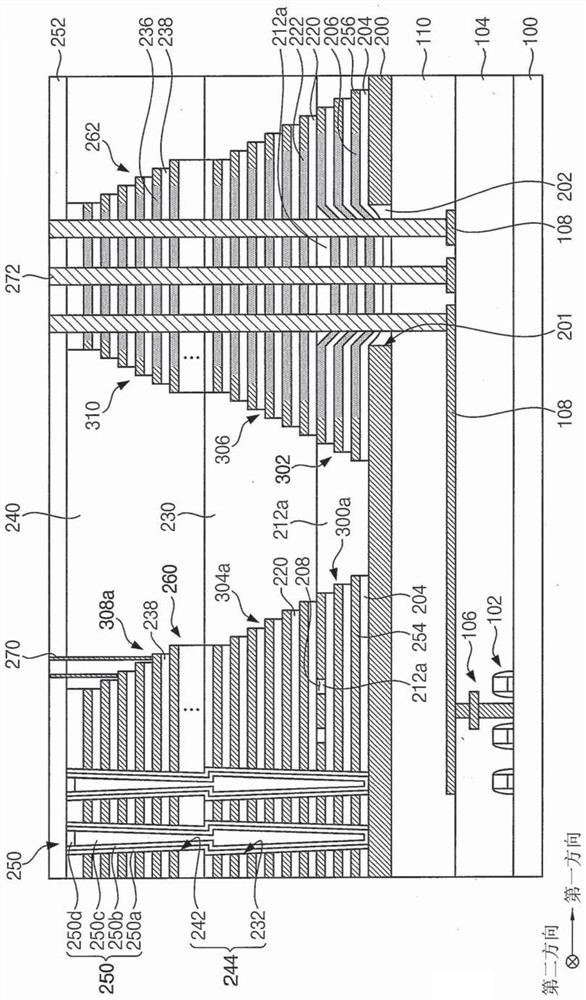
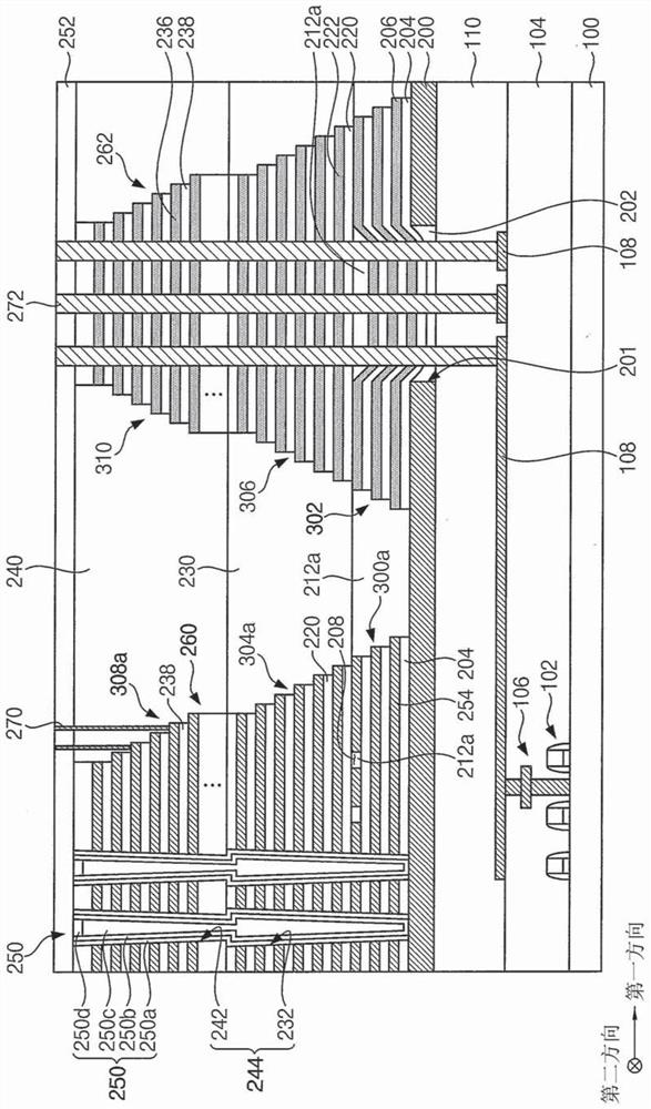
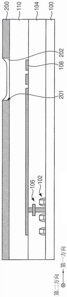
[0017] Hereinafter, a direction substantially perpendicular to the upper surface of the substrate is defined as a vertical direction, and two directions crossing each other in a horizontal direction substantially parallel to the upper surface of the substrate are defined as a first direction and a second direction, respectively. In example embodiments, the first direction and the second direction may be perpendicular to each other.

[0018] figure 1 is a cross-sectional view illustrating a vertical semiconductor device according to example embodiments. figure 2 is a cross-sectional view illustrating a vertical semiconductor device according to some example embodiments. refer to figure 1 , the vertical semiconductor device may include circuit patterns constituting peripheral circuits on the substrate 100 . In example embodiments, the circuit pattern may include a lower transistor 102 and a lower wiring 106 . The lower wiring 106 may include lower contact plugs and lower ...


PUM


Abstract

An integrated circuit device is disclosed. The integrated circuit device includes a vertical stack of non-volatile memory cells on a substrate, the vertical stack configured as a vertical NAND string of memory cells. Such vertical stack of non-volatile memory cells includes a plurality of gate patterns spaced apart from each other by corresponding electrically insulating layers. A dummy molding structure is also disposed on the substrate. The dummy molding structure includes a vertical stack having sacrificial layers spaced apart from each other by corresponding electrically insulating layers. An insulating pattern is provided that fills a recess in a recessed shape of a first sacrificial layer of the sacrificial layers in the vertical stack having the sacrificial layers. The insulating pattern has an upper surface coplanar with an upper surface of a first of the sacrificial layers.

Description

[0001] This application claims priority from Korean Patent Application No. 10-2020-0093215 filed on July 27, 2020, the contents of which are hereby incorporated by reference. technical field [0002] Example embodiments relate to integrated circuit devices, and more particularly, to integrated circuit devices having vertically and highly integrated semiconductor devices and methods of forming integrated circuit devices. Background technique [0003] As semiconductor devices become more highly integrated, VNAND flash memory devices may utilize a cell on periphery (COP) structure in which peripheral circuits are formed on a substrate and a cell stack structure including memory cells is stacked on the peripheral circuits. An insulating interlayer may be formed between the cell stack structures. As the height of the cell stack structure in the vertical direction increases, the planarization process of the upper surface of the insulating interlayer may be difficult. Therefore, r...

Claims


Application Information

Patent Timeline
Patent Type & Authority Applications(China)
IPC IPC(8): H01L27/11563H01L27/11578H01L27/1157
CPCH10B43/00H10B43/35H10B43/20H10B43/50H10B43/40H10B43/27
Inventor 黄昌善金己焕石韩率林钟欣张起硕
Owner SAMSUNG ELECTRONICS CO LTD
Why Eureka
Try Eureka