Scanning driving circuit, array substrate and display terminal

A scanning driving circuit and scanning driving technology, applied in static indicators, instruments, etc., can solve the problems of poor scanning signal accuracy and poor picture display effect, so as to solve the phenomenon of afterimage, improve the image display effect, enhance the stable effect

Active Publication Date: 2022-04-08
CHANGSHA HKC OPTOELECTRONICS CO LTD +1
View PDF7 Cites 5 Cited by
  • Summary
  • Abstract
  • Description
  • Claims
  • Application Information

AI Technical Summary

Problems solved by technology

However, since the clock signal is carried out according to a certain timing, there is a certain time delay between the multiple transmission signals and scanning signals output by one GOA unit, which leads to poor accuracy of scanning signal output and poor picture display effect

Method used

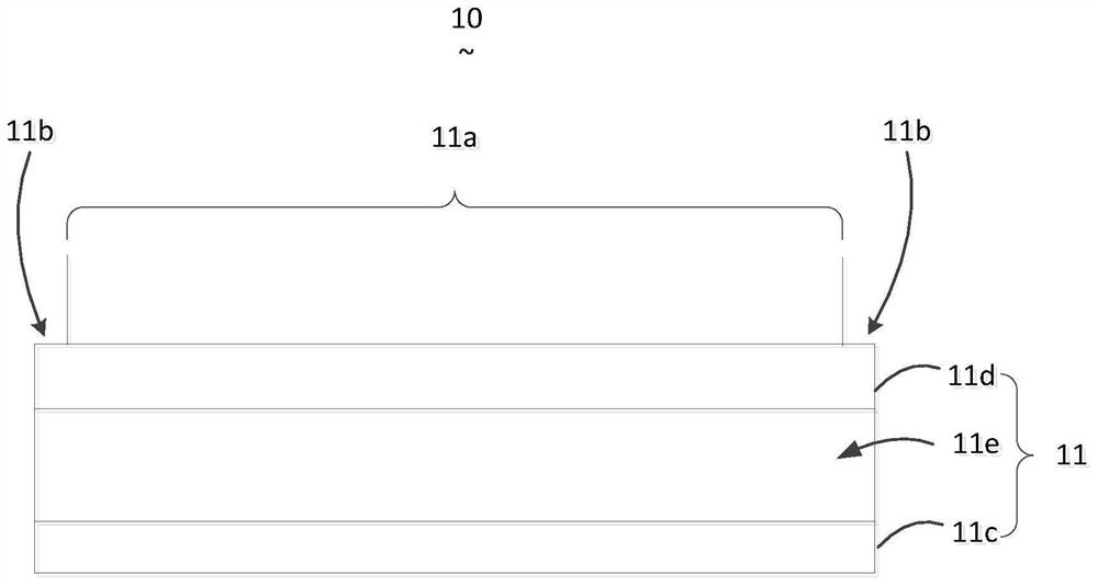
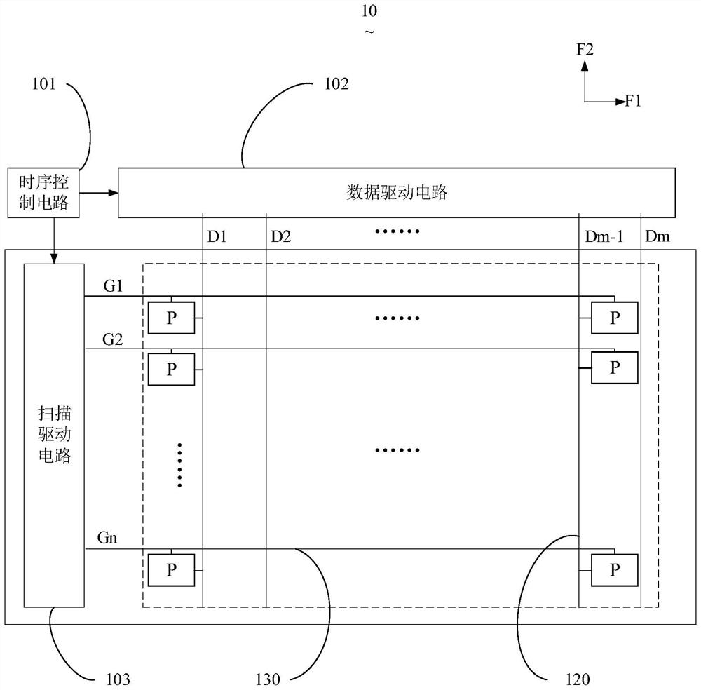
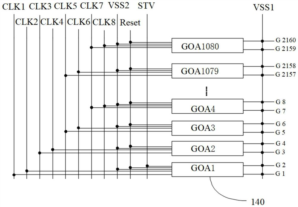

Image

  • Scanning driving circuit, array substrate and display terminal
  • Scanning driving circuit, array substrate and display terminal
  • Scanning driving circuit, array substrate and display terminal

Examples


Embodiment Construction

[0024] In order to facilitate the understanding of the present application, the present application will be described more fully below with reference to the relevant drawings. Preferred embodiments of the application are shown in the accompanying drawings. However, the present application can be embodied in many different forms and is not limited to the embodiments described herein. On the contrary, the purpose of providing these embodiments is to make the disclosure of the application more thorough and comprehensive.

[0025] The following descriptions of the various embodiments refer to the accompanying drawings to illustrate specific embodiments that the present application can be used to implement. The serial numbers assigned to components in this document, such as "first", "second", etc., are only used to distinguish the described objects, and do not have any sequence or technical meaning. The "connection" and "connection" mentioned in this application all include direc...


PUM


Abstract

The embodiment of the invention discloses a scanning driving circuit capable of accurately outputting scanning signals, which comprises n scanning driving units which are sequentially arranged and cascaded, and each scanning driving unit is used for outputting two scanning signals at an interval of preset time. Each scanning driving unit comprises two pull-down time adjusting modules which are used for adjusting the time of the scanning signal output end from the time of outputting the scanning signal to the time of stopping outputting the scanning signal to be the same. By adjusting the voltage drop time of the two scanning signals output by each scanning driving unit, the ghosting phenomenon during image display is reduced, and the image display effect is improved. The embodiment of the invention further discloses an array substrate comprising the scanning driving circuit and a display terminal.

Description

technical field [0001] The present application relates to the field of display technology, in particular to a scan driving circuit, an array substrate and a display terminal applied to a display panel. Background technique [0002] At present, most liquid crystal display panels adopt the gate driver on array (Gate Driver on Array, GOA) technology. The GOA technology uses the thin film transistor (Thin Film Transistor, TFT) liquid crystal display array process to manufacture the gate scanning drive circuit on the thin film transistor array. On the substrate, to realize the driving technology of progressive scanning, which has the advantages of reducing the production cost and realizing the narrow frame of the panel. [0003] Currently, among the cascaded GOA units, one GOA unit can output two or more cascading signals and scanning signals under the control of a clock signal (Clock, CLK). However, since the clock signal is carried out according to a certain timing, there is a...

Claims


Application Information

Patent Timeline
Patent Type & Authority Applications(China)
IPC IPC(8): G09G3/36
CPCY02D10/00
Inventor 金秉勋卢昭阳曹尚操田尚益李荣荣
Owner CHANGSHA HKC OPTOELECTRONICS CO LTD
Why Eureka
Try Eureka